Semiconductor laser device protection circuit, optical pickup apparatus, and information recording/reproducing apparatus

a laser device and protection circuit technology, applied in semiconductor lasers, optical beam sources, instruments, etc., can solve the problems that the laser diode cannot be protected, and achieve the effects of avoiding leak current flow, improving yield, and being more reliabl

Inactive Publication Date: 2011-05-31
SHARP KK
View PDF7 Cites 8 Cited by
  • Summary
  • Abstract
  • Description
  • Claims
  • Application Information

AI Technical Summary

Benefits of technology

[0012]An object of the invention is to provide a semiconductor laser device protection circuit which can protect a semiconductor laser device from static electricity and leak current and eliminate the need for releasing a short-circuited state, and to provide an optical pickup apparatus and information recording / reproducing apparatus including the same.
[0039]Accordingly, the short-circuited state can be removed by adjusting the voltage that is applied to the base, to be lower than the predetermined voltage, thereby excluding the work for removing the short-circuited state. Because of no need to use the soldering iron for removing the short-circuited state, it is also possible to avoid the leak current flow. Consequently, the semiconductor laser device can be improved in yield, and the semiconductor laser device mounted can be more reliable. In addition, the productivity can also be increased since the work for removing the short-circuited state can be excluded.
[0040]The optical pickup apparatus may include the aforementioned optical module. In this case, there is no need to provide a space in which the semiconductor laser device protection circuit is mounted, separately, with the result that the optical pickup apparatus can be downsized.
[0041]According to the invention, the information recording / reproducing apparatus uses the aforementioned optical pickup apparatus to record or reproduce information on an optical recording medium, with the result that the information recording / reproducing apparatus itself is not required to take any measures against static electricity to protect the semiconductor laser device.

Problems solved by technology

A problem may arise during the use of a soldering iron in the soldering work and solder removal because leak current may possibly flow through the semiconductor laser device due to a ground failure caused by the soldering iron.
In the technique disclosed by JP-U 6-52018, although no current over the maximum rated value flows through the laser diode which can be thus prevented from breakage, there is a problem that electricity needs to be supplied also to the laser diode protection circuit and unless electricity is supplied to the optical pickup apparatus, the semiconductor laser device such as the laser diode cannot be protected.

Method used


Image

  • Semiconductor laser device protection circuit, optical pickup apparatus, and information recording/reproducing apparatus
  • Semiconductor laser device protection circuit, optical pickup apparatus, and information recording/reproducing apparatus
  • Semiconductor laser device protection circuit, optical pickup apparatus, and information recording/reproducing apparatus

Examples


Embodiment Construction

[0048]Now referring to the drawings, preferred embodiments of the invention are described below.

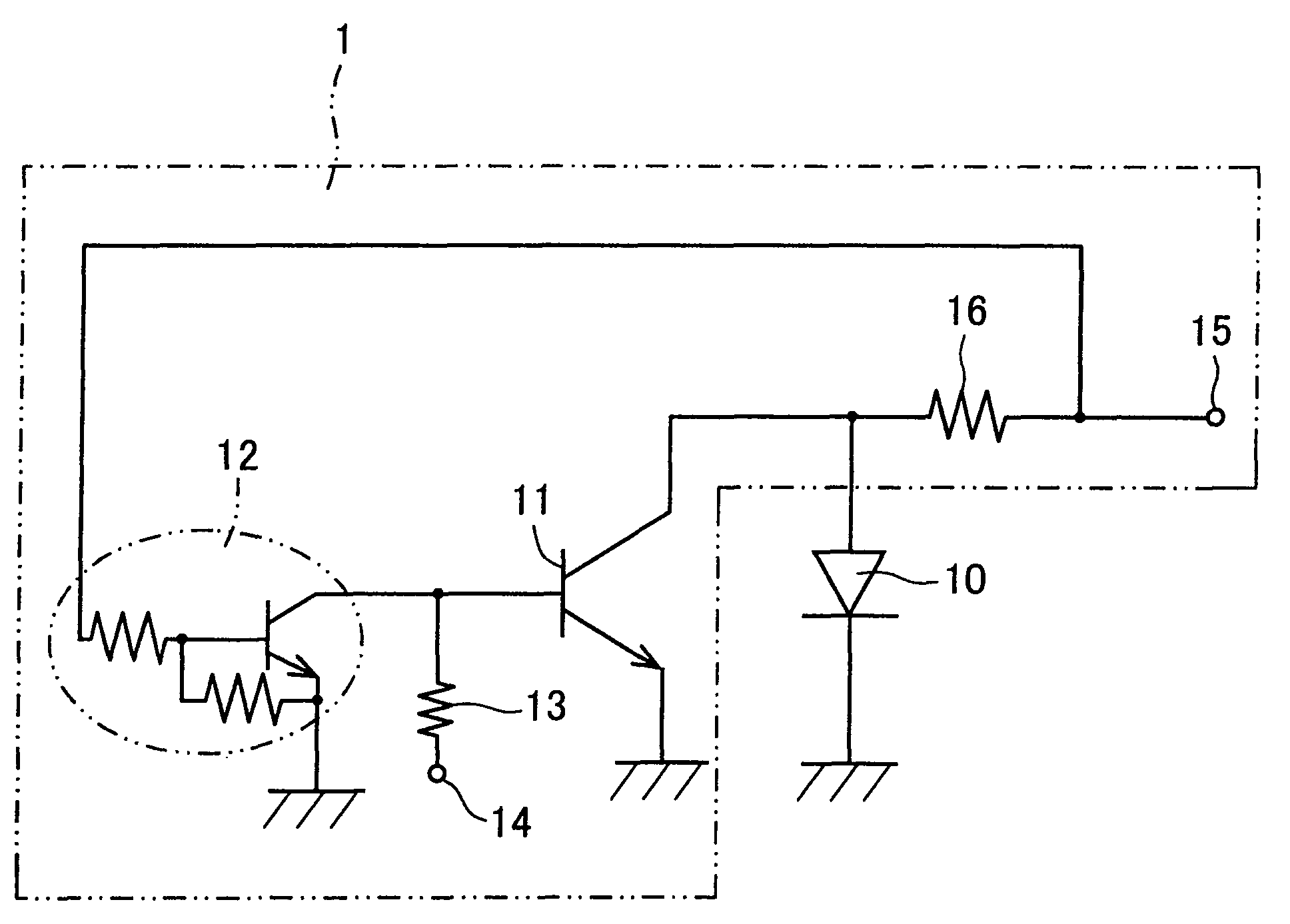
[0049]FIG. 1 is a view showing a configuration of an electrical switching circuit 1 according to one embodiment of the invention. The electrical switching circuit 1 serving as a semiconductor laser device protection circuit includes a transistor 11, a digital transistor 12, a first resistor 13, a first external terminal 14, a second external terminal 15, and a second resistor 16.

[0050]A semiconductor laser device 10 is composed of a laser diode, for example. The semiconductor laser device 10 has a cathode grounded and an anode connected to the transistor 11. The transistor 11 serving as a transistor is an npn bipolar transistor and has a collector connected to the cathode of the semiconductor laser device 10, an emitter grounded, and a base connected to the first external terminal 14 via the first resistor 13. The first resistor 13 is composed of a carbon resistor, for example, and has re...


PUM

PropertyMeasurementUnit
voltageaaaaaaaaaa
voltageaaaaaaaaaa
voltageaaaaaaaaaa

Abstract

A semiconductor laser device has a cathode grounded and an anode connected to a collector of a transistor. The transistor has an emitter grounded and a base connected to a first external terminal via a first resistor. A digital transistor has a collector connected to the base of the transistor, an emitter grounded, and a base connected to a second external terminal via a resistor. When a voltage equal to or higher than the predetermined first voltage is applied to the base of the transistor, the transistor is put into a conducting state, and the semiconductor laser device is grounded via the transistor and thereby protected from static electricity and leak current.

Description

CROSS-REFERENCE TO RELATED APPLICATION[0001]This application claims priority to Japanese Patent Application No. 2007-278036, which was filed on Oct. 25, 2007, the contents of which are incorporated herein by reference in its entirety.BACKGROUND OF THE INVENTION[0002]1. Field of the Invention[0003]The present invention relates to a semiconductor laser device protection circuit capable of protecting a semiconductor laser device from being broken by static electricity, and to an optical pickup apparatus and information recording / reproducing apparatus including the same. More particularly, the present invention relates to a semiconductor laser device protection circuit capable of protecting a semiconductor laser device that is used to record / reproduce information on a disk-shaped optical recording medium such as an optical disk or a magneto-optical disk from being broken by static electricity, and to an optical pickup apparatus and an information recording / reproducing apparatus which in...

Claims


Application Information

Patent Timeline
Patent Type & Authority Patents(United States)
IPC IPC(8): G11B7/00
CPCG11B7/121H01S5/042G11B7/126H01S5/06825
Inventor SUZUKI, HIROFUMI
Owner SHARP KK
Why Eureka
Try Eureka