Capacitive sensor
a capacitive sensor and capacitive technology, applied in the direction of instruments, diagnostic recording/measure, force/torque/work measurement apparatus, etc., can solve the problem that the electrode is unlikely to peel away from the dielectric layer, and achieve the effect of favorable conductivity, high conductivity, and favorable conductivity
- Summary
- Abstract
- Description
- Claims
- Application Information
AI Technical Summary
Benefits of technology
Problems solved by technology
Method used
Image
Examples
first embodiment
[0106]An embodiment of the first capacitive sensor according to the present invention will be hereinafter described. Note that embodiments of the first capacitive sensor according to the present invention are not limited to this embodiment, and the first capacitive sensor according to the present invention may be implemented in various modified and improved embodiments possible to a person skilled in the art.
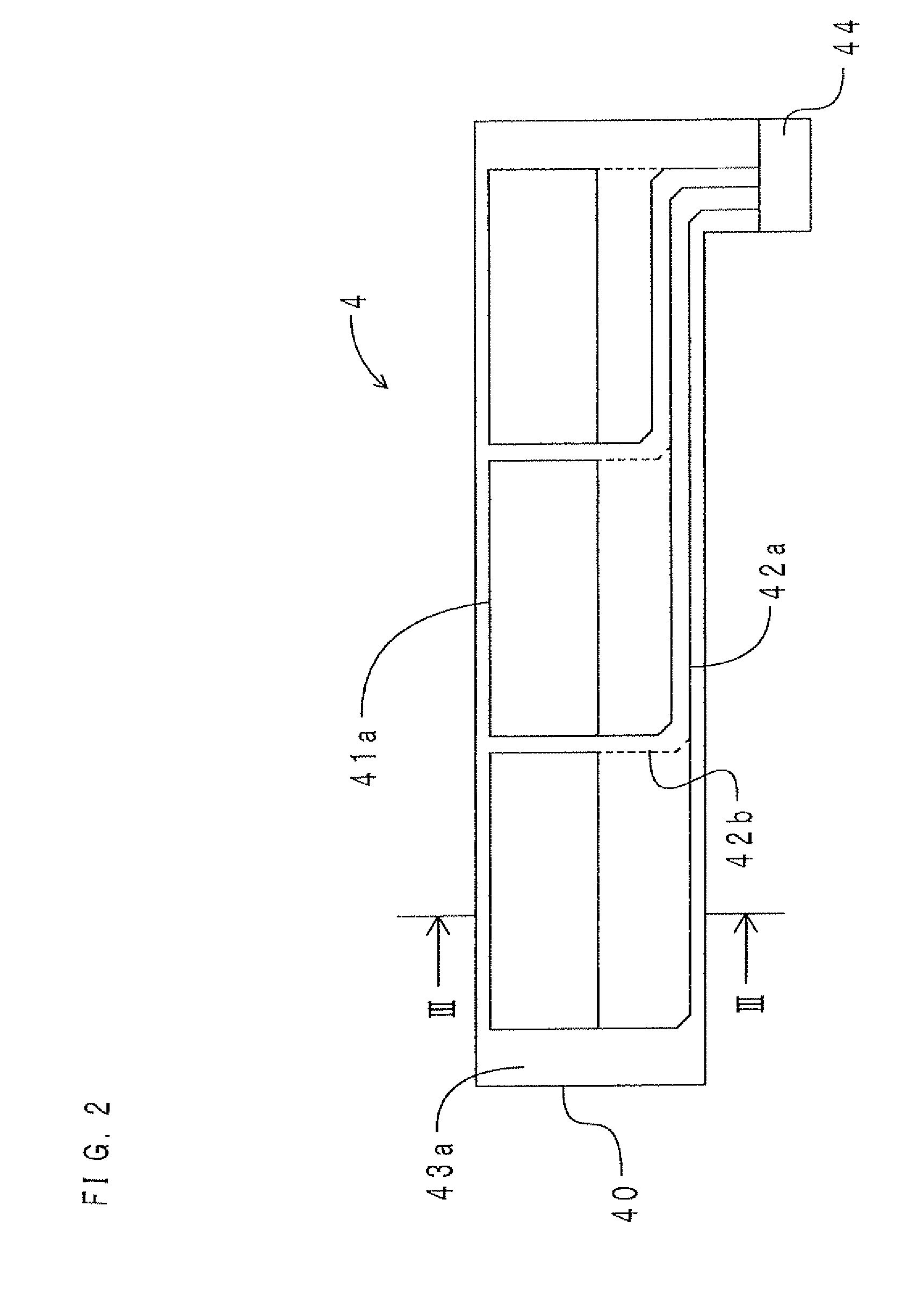
[0107]First, the constitution of the capacitive sensor according to this embodiment will be described. FIG. 2 is a top view of the capacitive sensor. FIG. 3 is a sectional view taken along the line III-III of FIG. 2. As shown in FIGS. 2 and 3, a capacitive sensor 4 includes a dielectric layer 40, a pair of electrodes 41a, 41b, conductors 42a, 42b, and cover films 43a, 43b.
[0108]The dielectric layer 40 is made from urethane rubber and takes a belt shape extending in a left-right direction. The thickness of the dielectric layer 40 is approximately 300 μm.
[0109]The electrode 41a t...
second embodiment
[0117]A capacitive sensor according to this embodiment differs from the capacitive sensor according to the first embodiment by the constitution in which the electrodes and the conductors are formed on the elastic substrate, instead of the dielectric layer. Therefore, only this difference will be hereinafter described.
[0118]FIG. 4 is a top view of the capacitive sensor according to this embodiment. FIG. 5 is a sectional view taken along the line V-V of FIG. 4. Note that, for ease of description, an upper elastic substrate is shown as being transparent in FIG. 4. Further, in FIG. 5, a gap between the upper elastic substrate and a dielectric layer and a gap between a lower elastic substrate and the dielectric layer are emphasized for ease of description.
[0119]As shown in FIGS. 4 and 5, a capacitive sensor 5 includes a dielectric layer 50, a pair of electrodes 51a, 51b, conductors 52a, 52b, an upper elastic substrate 53a, and a lower elastic substrate 53b.
[0120]The upper elastic substr...
third embodiment
[0123][Constitution]
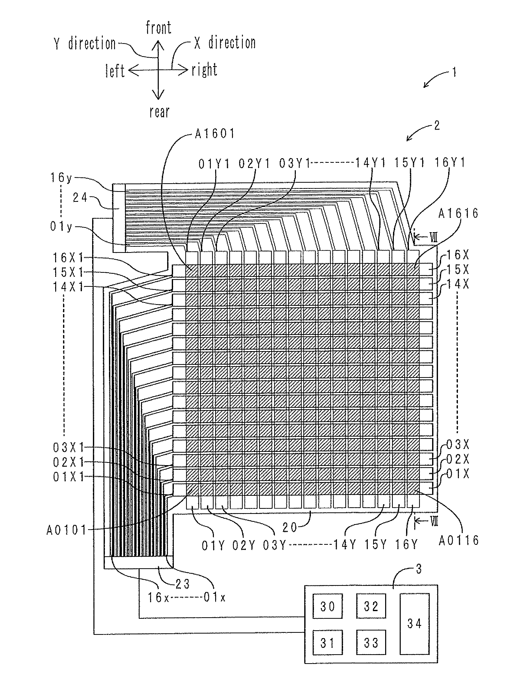
[0124]First, the constitution of a capacitive sensor according to this embodiment will be described. FIG. 6 is a perspective top view of the capacitive sensor according to this embodiment. Note that in FIG. 6, a surface side insulating cover layer and a back side insulating cover layer have been omitted. Further, a back side electrode and a back side conductor are indicated by thin lines, and detection portions are shown as the hatched portions. FIG. 7 is a sectional view taken along the line VII-VII of FIG. 6. Note that in FIG. 7, the thickness of a sensor main body in an up-down direction is emphasized. As shown in FIGS. 6 and 7, a capacitive sensor 1 according to this embodiment includes a sensor main body 2 and a calculation portion 3.
[0125]The sensor main body 2 includes a dielectric layer 20, surface side electrodes 01X to 16X, back side electrodes 01Y to 16Y, detection portions A0101 to A1616, surface side conductors 01x to 16x, back side conductors 01y to...
PUM
| Property | Measurement | Unit |
|---|---|---|
| impedance measurement | aaaaa | aaaaa |
| surface area | aaaaa | aaaaa |
| specific dielectric constant | aaaaa | aaaaa |
Abstract
Description
Claims
Application Information
 - R&D
- Intellectual Property
- Life Sciences
- Materials
- Tech Scout
- Unparalleled Data Quality
- Higher Quality Content
- 60% Fewer Hallucinations
Browse by: Latest US Patents, China's latest patents, Technical Efficacy Thesaurus, Application Domain, Technology Topic, Popular Technical Reports.
© 2025 PatSnap. All rights reserved.Legal|Privacy policy|Modern Slavery Act Transparency Statement|Sitemap|About US| Contact US: help@patsnap.com


