Electronic device and method of manufacturing the same

a manufacturing method and electronic technology, applied in the direction of semiconductor devices, basic electric elements, electrical equipment, etc., can solve the problems of difficult application of light and flexible resin substrates, relatively long processing time, energy efficiency, etc., to improve the mobility of carriers and improve the on/off ratio, the effect of improving the production efficiency and the property

Inactive Publication Date: 2011-06-28
KONICA MINOLTA INC
View PDF2 Cites 26 Cited by
  • Summary
  • Abstract
  • Description
  • Claims
  • Application Information

AI Technical Summary

Benefits of technology

[0019]An object of the present invention is to improve the production efficiency and the property of an electronic device, specifically, a thin film transistor, and more concretely, to improve the carrier mobility and the on / off ratio thereof.

Problems solved by technology

However, in the usual thermal oxidation method, since the treatment is carried out in a very high temperature range of 400° C. or more, the energy efficiency is not high, a relatively long processing time is needed, and the application of a light and flexible resin substrate becomes difficult because the temperature of the substrate increases as high as the treatment temperature.
In the case of plasma oxidation, since the treatment is carried out in an extremely reactive plasma space, there has been a problem that the electrode or the insulating layer is more degraded in the thin film transistor manufacturing process whereby the mobility and the off electric current (dark current) turns worse.
Accordingly, a high production efficiency is difficult to obtain because the electrode forming process and the insulating layer forming process is separated.
Further, the drying of the insulating layer takes time because it is dried by external heating.
Further, a high production efficiency is difficult to obtain because the electrode forming process and the insulating layer forming process is separated.
In Patent Document 5, a production process of an insulating layer via an atmospheric pressure plasma CVD method is disclosed, where, also, a high production efficiency is difficult to obtain because the electrode forming process and the insulating layer forming process is obviously separated.
However, this method has problems in that the productivity and the material efficiency are not high because the DLC layer is formed under vacuum and the DLC layer which is fundamentally unnecessary must be removed.

Method used


Image

  • Electronic device and method of manufacturing the same
  • Electronic device and method of manufacturing the same
  • Electronic device and method of manufacturing the same

Examples


example 1

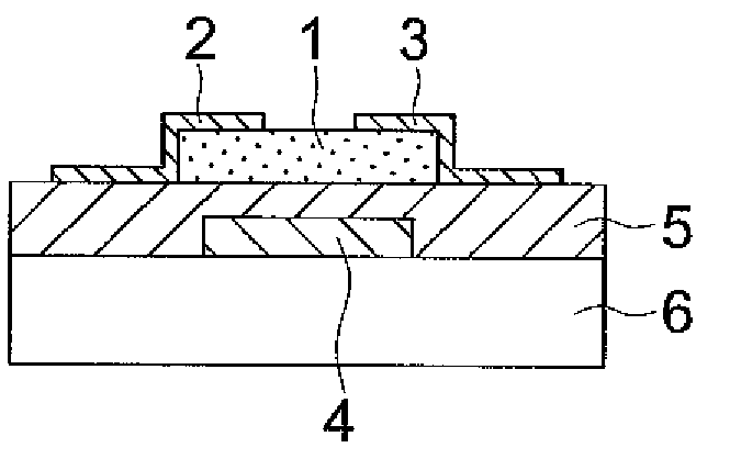
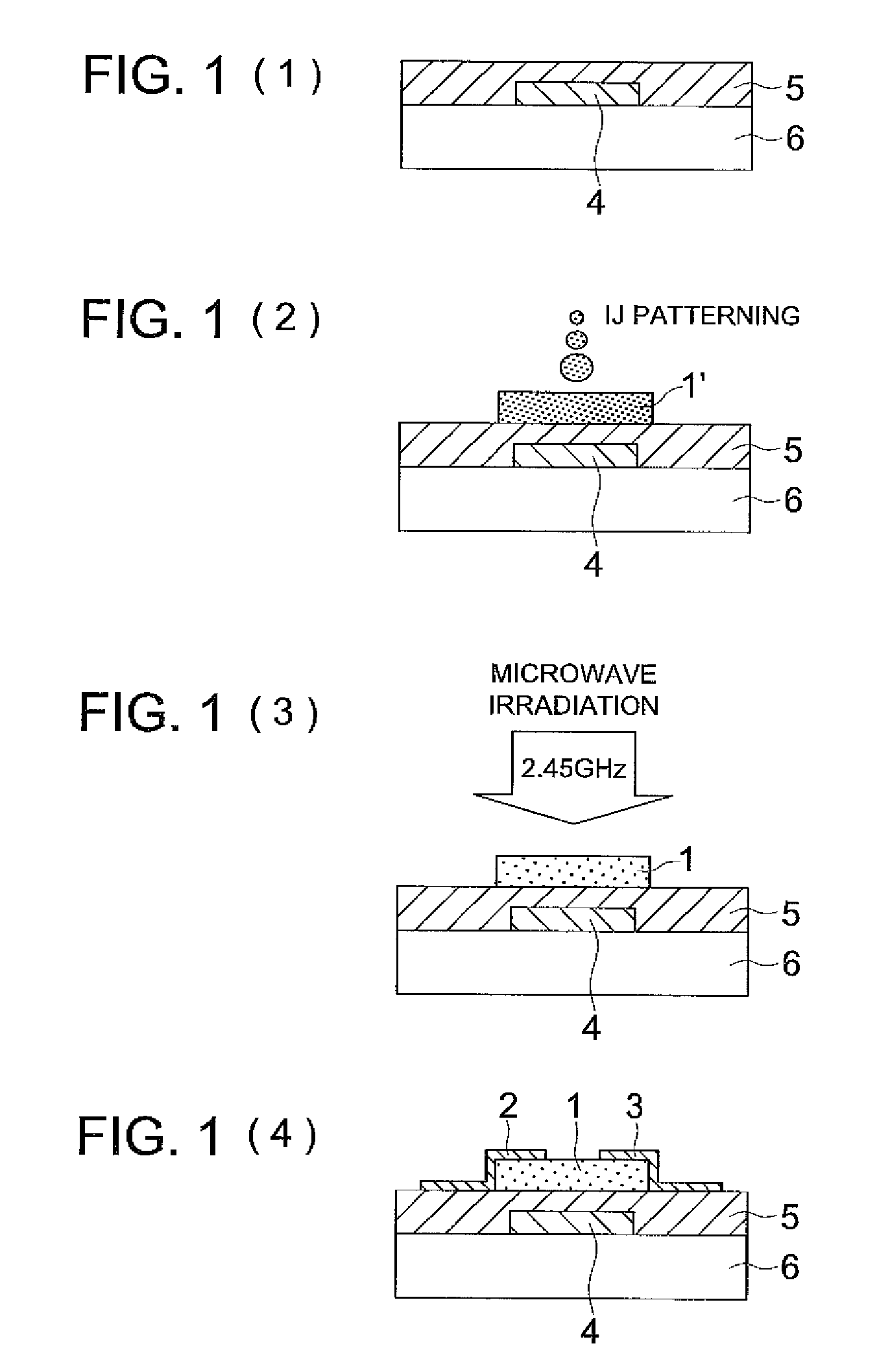
Example of Thin Film Transistor Having Bottom Gate-Top Contact Structure

[0291]In FIGS. 1(1)-1(4), schematic cross-sectional views illustrating the manufacturing process are shown.

[0292]As substrate 6, a glass substrate was used, and an ITO film was formed on the substrate by sputtering. Then, the ITO film was subjected to patterning to form gate electrode 4 (100 nm in thickness).

[0293]Subsequently, gate insulation layer 5 constitute of 200 nm thick silicon oxide was formed by an atmospheric pressure plasma CVD method (FIG. 1(1)). The atmospheric pressure plasma treatment apparatus disclosed in FIG. 6 of JP-A No. 2003-303520 was used.

(Gases Used)

[0294]Inert gas: helium 98.25% by volume

[0295]Reactive gas: oxygen gas 1.5% by volume

[0296]Reactive gas: tetraethoxysilane vapor (bubbled with helium gas) 0.25% by volume

(Discharge Conditions)

[0297]High frequency power source: 13.56 MHz

[0298]Discharge power: 10 W / cm2

(Electrode Conditions)

[0299]The electrode is a grounded roll electrode havin...

example 2

Manufacturing of Thin Film Transistor 201

[0306]A transistor was Manufactured in the same manner as in Example 1.

(Formation of Semiconductor Precursor Thin Film)

[0307]Indium nitrate, zinc nitrate and gallium nitrate were mixed in a molar ratio of 1:0.1:0.5 and dissolved in water (a mixture of water / ethanol=9 / 1 in mass ratio) to form a 10 mass % aqueous solution, which was then used as an ink for inkjet printing to eject the solution onto a channel formation area, followed by drying by heating at 150° C. for 10 minutes to form semiconductor precursor material thin film 1′ was formed (FIG. 1(2)).

[0308]By conducting microwave irradiation under the same condition as in Example 1, semiconductor precursor material thin film 1′ was transformed into semiconductor layer 1 in the same way as above due to the thermal oxidation with the heat transferred from the electrode.

[0309]Subsequently, the source electrode and the drain electrode were formed in the same manner as in Example 1 to obtain thi...
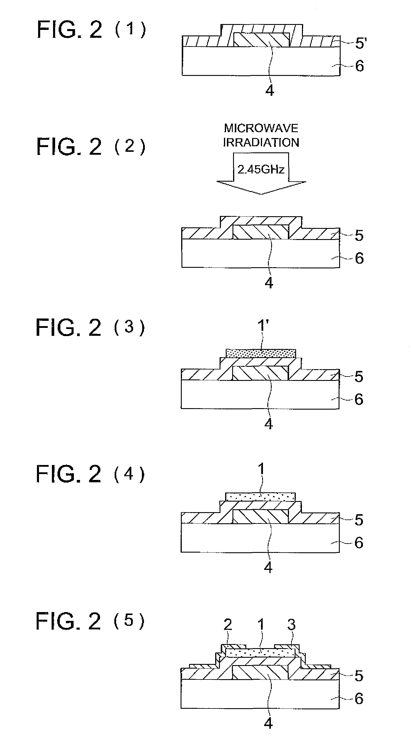
example 3

[0331]In FIGS. 2(1)-2(5), schematic cross-sectional views illustrating the manufacturing process are shown.

[0332]As substrate 6, a glass substrate was used, and an ITO film was formed on the substrate by sputtering. Then, the ITO film was subjected to patterning to form gate electrode 4 (100 nm in thickness).

[0333]Next, Aqua Micah NN110 (perhydropolysilazane / xylene solution: produced by AZ Electronic Materials) was applied on the substrate by a spin coat method (3000 rpm×30 sec), followed by drying to obtain insulating film precursor layer 5′ (200 nm in thickness). FIG. 2(1)

[0334]Microwave irradiation was carried out in the same manner as in Example 1, namely, Next, Aqua Micah NN110 (perhydropolysilazane / xylene solution: produced by AZ Electronic Materials) was applied on the substrate by a spin coat method (3000 rpm×30 sec), followed by drying to obtain insulating film precursor layer 5′ was formed (200 nm in thickness). FIG. 2(1)

[0335]Microwave irradiation was carried out in the s...


PUM

PropertyMeasurementUnit
temperatureaaaaaaaaaa

Abstract

A method of manufacturing an electronic device comprising the subsequent steps of: providing a thermal conversion material or an area comprising the thermal conversion material and, in an adjoining area or in a vicinity of the thermal conversion material or the area comprising the thermal conversion material, a material having an electromagnetic wave absorbing function or an area comprising the material having the electromagnetic wave absorbing function, in at least a portion on a substrate; and irradiating the substrate with an electromagnetic wave to transform the thermal conversion material into a functional material using a heat generated by the material having the electromagnetic wave absorbing function.

Description

FIELD OF THE INVENTION[0001]The present invention relates to a method of manufacturing an electronic device with a high efficiency, by which a plurality of functional films, for example, an electrode, an insulating layer and a semiconductor layer are simultaneously formed using a substance having an electromagnetic wave absorbing function and, in more detail, relates to a method of manufacturing an electronic device with a high production efficiency, by which manufacturing via a coating process (for example, printing and IJ) and one process manufacturing of simultaneously forming an electrode and a semiconductor are capable.BACKGROUND OF THE INVENTION[0002]As a technology to oxidize a metal film to transform the metal film into a metal oxide semiconductor film, an attempt to oxidize a metal film such as Cu, Zn, Al formed on a substrate through thermal oxidation or plasma oxidation to transform the metal film into a metal oxide semiconductor film has been conducted (for example, refe...

Claims


Application Information

Patent Timeline
Patent Type & Authority Patents(United States)
IPC IPC(8): H01L21/00H01L21/84
CPCH01L29/7869H01L51/0008H01L51/0545H01L51/0094H01L51/0541H01L51/0055H10K71/16H10K85/623H10K10/464H10K85/40H10K10/466
Inventor HONDA, MAKOTOHIRAI, KATSURA
Owner KONICA MINOLTA INC
Why Eureka
Try Eureka