

Hole inspection apparatus and hole inspection method using the same
a technology for inspecting apparatus and via holes, which is applied in the direction of semiconductor/solid-state device testing/measurement, instruments, nuclear engineering, etc., can solve the problems of reducing the accuracy of data about the holes, reducing the danger of damage to samples, and reducing the time taken.
- Summary
- Abstract
- Description
- Claims
- Application Information
AI Technical Summary
Benefits of technology
Problems solved by technology
Method used
Image

Examples
Embodiment Construction
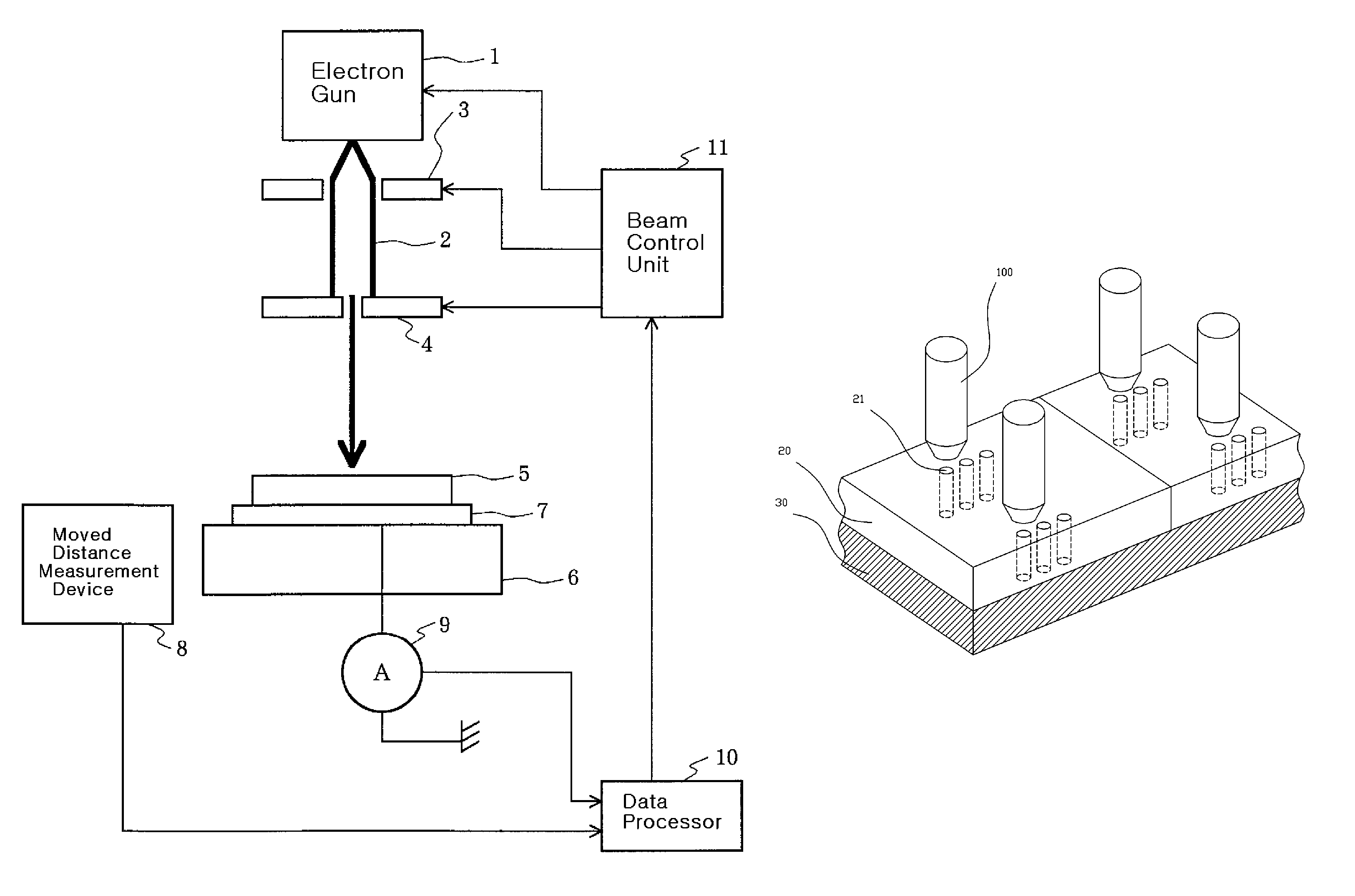
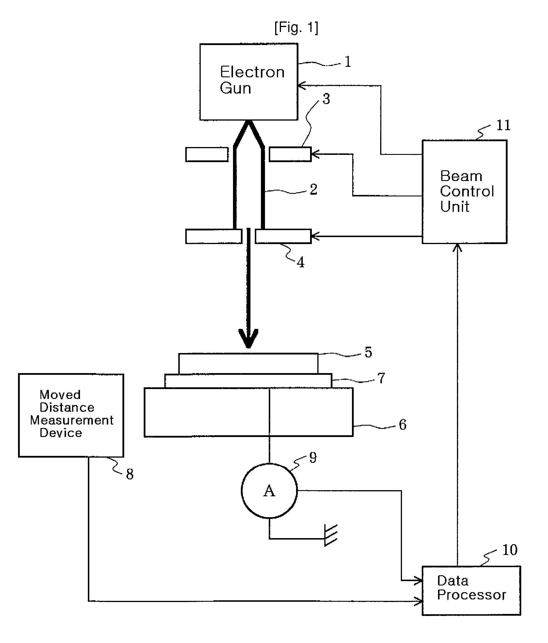
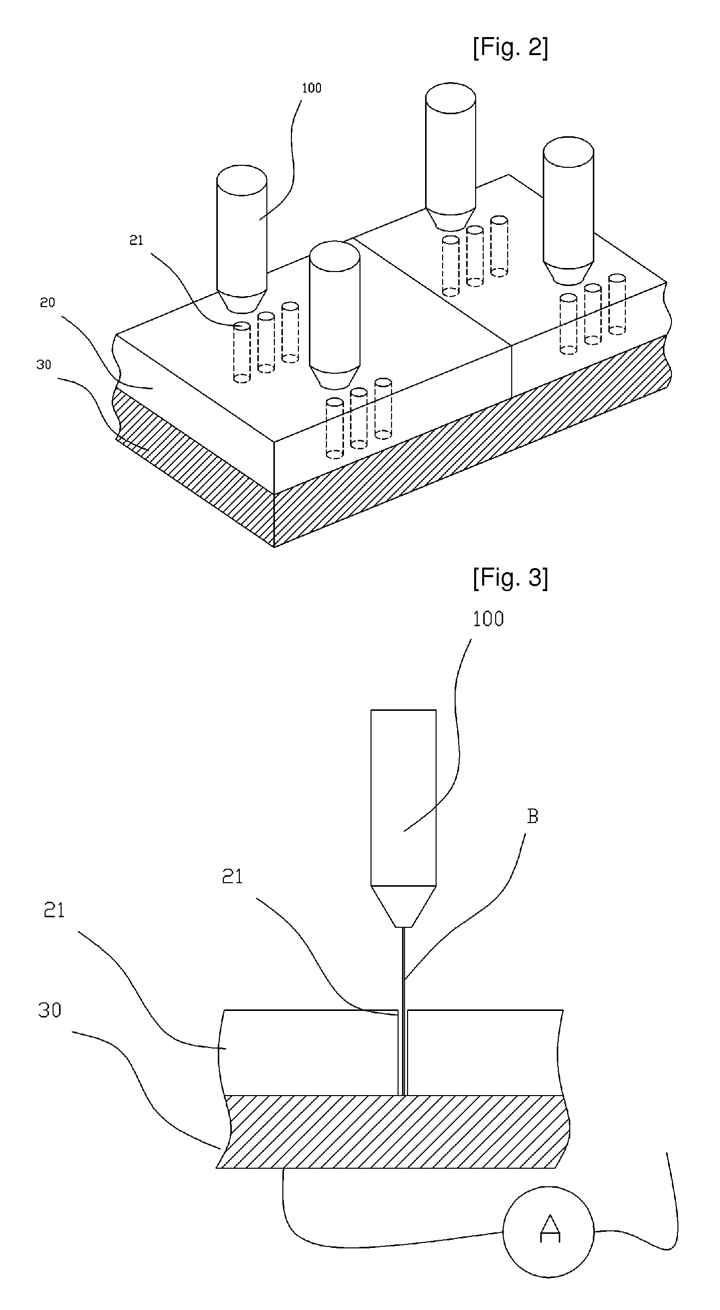
[0027]FIG. 2 is a perspective view schematically showing a hole inspection apparatus according to the present invention.
[0028]In FIG. 2, four electron columns 100 are used as electron beam irradiation means. For each of description, each electron column 100 is described as irradiating an electron beam across three holes 21. The holes 21 are formed in an insulating layer 20. A conductive layer 30 is located under the insulating layer 20. In this case, the three holes 21 to be inspected by each electron column 100 are formed in the insulating layer 20. Although the number of holes 21 and the size and shape of each hole have been set for the sake of description of the inspection apparatus according to the present invention, the number of holes 21 and the size and shape of each hole may be variously determined.
[0029]As shown in FIG. 2, the insulating layer 20 is divided into two regions, and the conductive layer 30 located under the insulating layer 20 is formed of a single layer. Accor...
PUM
 Abstract
Description
Claims
Application Information