Quasi-vertical gated NPN-PNP ESD protection device

a protection device and quasi-vertical gate technology, applied in semiconductor devices, diodes, electrical equipment, etc., can solve the problems of continuing electrostatic discharge (esd)

Active Publication Date: 2011-06-28
TEXAS INSTR INC
View PDF2 Cites 18 Cited by
  • Summary
  • Abstract
  • Description
  • Claims
  • Application Information

AI Technical Summary

Benefits of technology

[0007]The device can be used as a self-protecting QVDEMOS device at an I/O which allows sparing the area of an additional ES

Problems solved by technology

Electrostatic discharge (ESD) is a continuing problem in the design, manufacture and utilization of semiconductor devices.
Such E

Method used


Image

  • Quasi-vertical gated NPN-PNP ESD protection device
  • Quasi-vertical gated NPN-PNP ESD protection device
  • Quasi-vertical gated NPN-PNP ESD protection device

Examples


Embodiment Construction

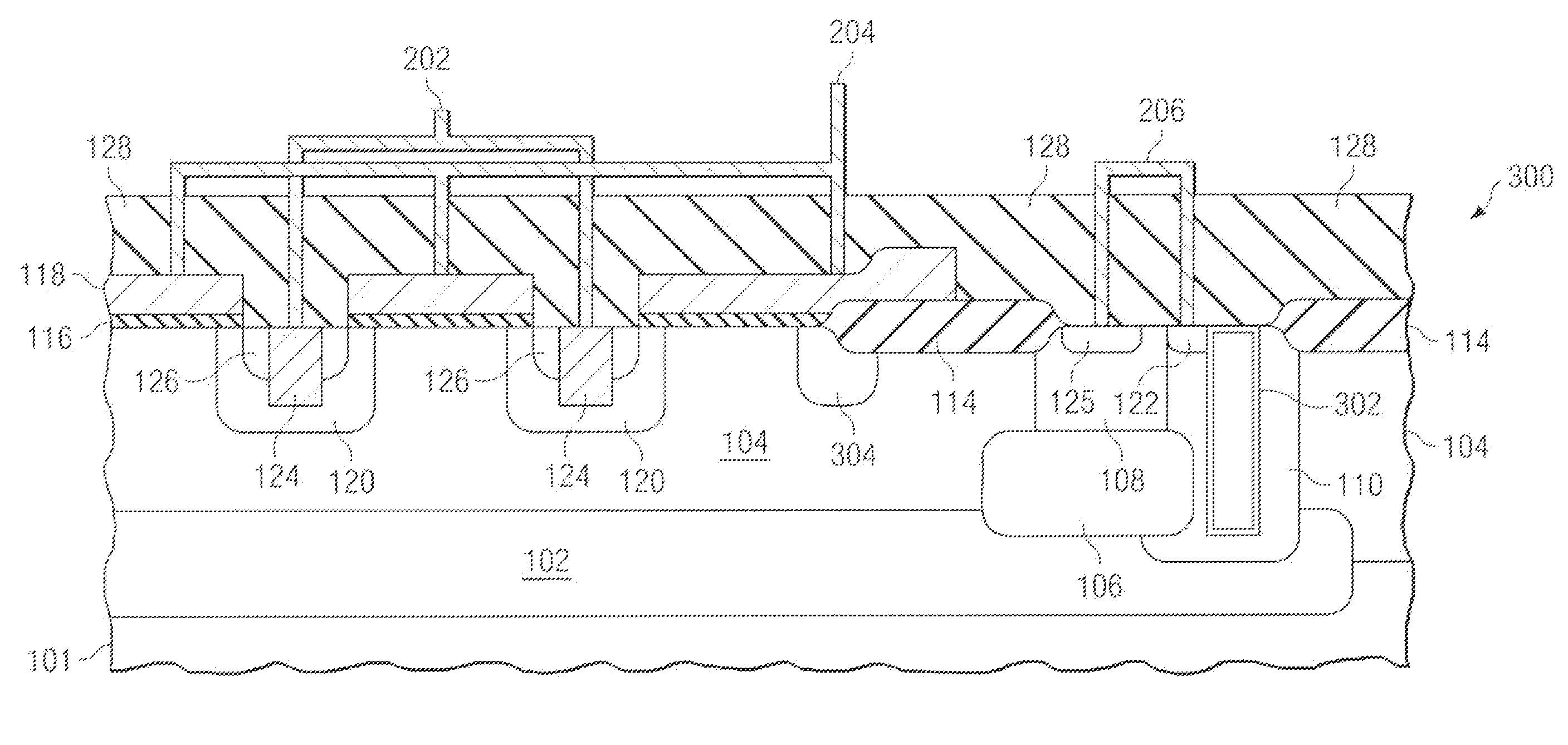
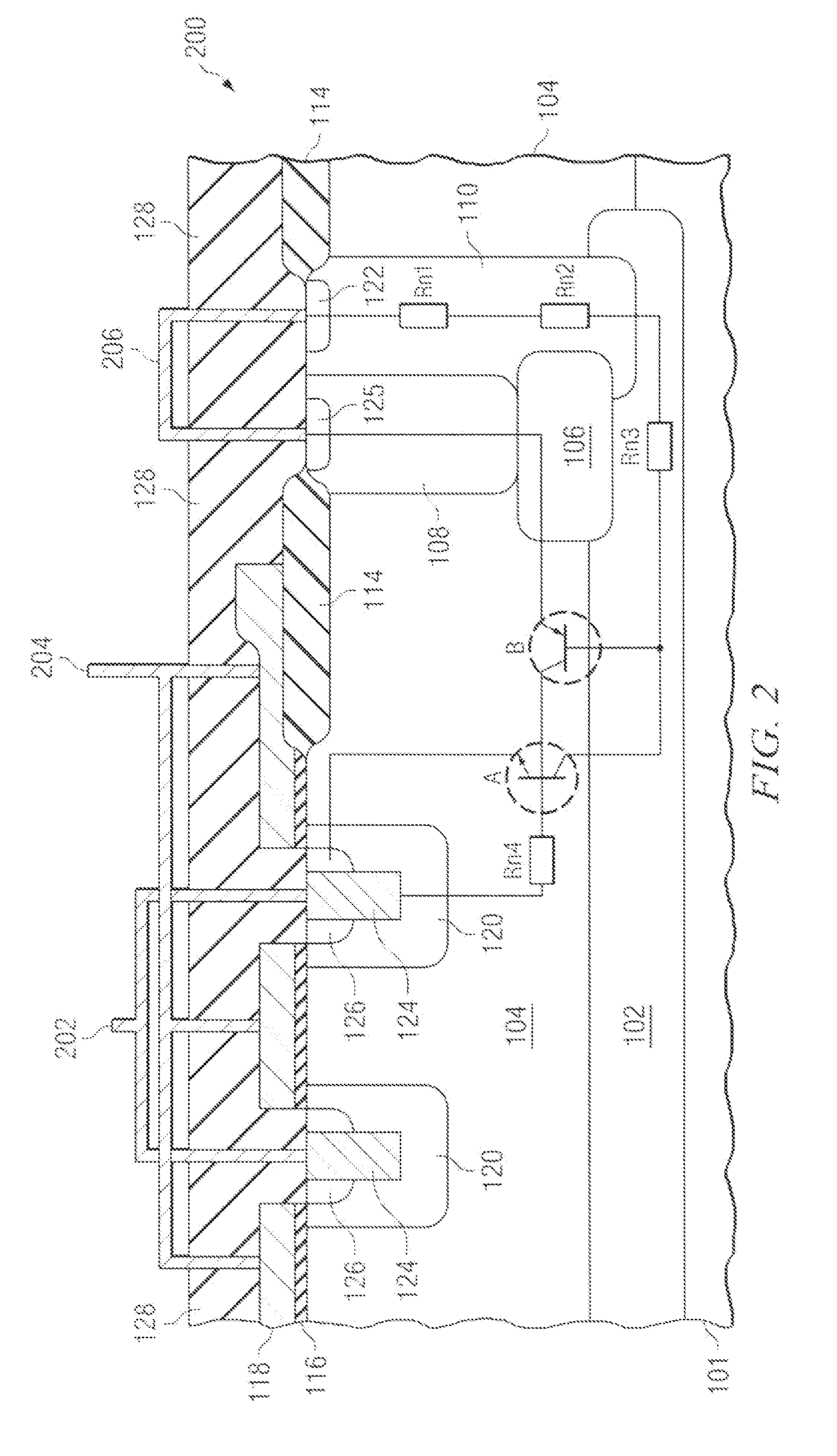
[0021]The description herein is made with reference to the drawings, wherein like reference numerals are generally utilized to refer to like elements throughout, and wherein the various structures are not necessarily drawn to scale. In the following description, for purposes of explanation, numerous specific details are set forth in order to facilitate understanding. It may be evident, however, to one skilled in the art, that one or more aspects described herein may be practiced with a lesser degree of these specific details. In other instances, known structures and devices are shown in block diagram form to facilitate understanding.

[0022]In the examples of this disclosure, it is supposed that semiconductor regions are doped using either dopant implantation or deposition of a doped material at the surface of the semiconductor material followed by diffusion into the semiconductor material. Patterned doped regions are assumed to be obtained by means of traditional lithographic techniq...


PUM


Abstract

Fashioning a quasi-vertical gated NPN-PNP (QVGNP) electrostatic discharge (ESD) protection device is disclosed. The QVGNP ESD protection device has a well having one conductivity type formed adjacent to a deep well having another conductivity type. The device has a desired holding voltage and a substantially homogenous current flow, and is thus highly robust. The device can be fashioned in a cost effective manner by being formed during a BiCMOS or Smart Power fabrication process.

Description

FIELD[0001]The disclosure herein relates generally to designing and fabricating a semiconductor quasi-vertical gated NPN-PNP electrostatic discharge (ESD) protection device.BACKGROUND[0002]Electrostatic discharge (ESD) is a continuing problem in the design, manufacture and utilization of semiconductor devices. A major source of ESD exposure to ICs is from the human body (described by the “Human Body Model”, HBM). In this situation, a packaged IC acquires a charge when it is held by a human who is electrostatically charged (e.g., from walking across carpeting). A charge of about 0.6 μC can be induced on a body capacitance of 150 pF, for example, leading to electrostatic potentials of 4 kV or greater and discharging peak currents of several amperes to the IC for about 100 ns, for example. A second source of ESD is from metallic objects (described by the “Machine model”, MM), which is characterized by a greater capacitance, lower internal resistance and transients that have significant...

Claims


Application Information

Patent Timeline
IPC IPC(8): H01L29/66
CPCH01L27/0262H01L29/66121H01L29/7436H01L29/87H01L29/66393H01L29/0696
Inventor DENISON, MARIEHAO, PINGHAI
Owner TEXAS INSTR INC
Why Eureka
Try Eureka