
Semiconductor Device and Method for Manufacturing the Same

a semiconductor device and manufacturing method technology, applied in the field of semiconductor devices, can solve the problems of reduced manufacturing yield, increased manufacturing cost, and disadvantageous high-speed operation of transistors, and achieve the effects of reducing manufacturing costs, increasing manufacturing yield, and improving reliability of semiconductor device characteristics

Active Publication Date: 2011-11-03
UNIV OF ZAGREB FACULTY OF ELECTRICAL ENG & COMPUTING
View PDF4 Cites 16 Cited by
  • Summary
  • Abstract
  • Description
  • Claims
  • Application Information

AI Technical Summary

Benefits of technology

"The present invention relates to a semiconductor device and a method for manufacturing the semiconductor device. More specifically, the invention is about a semiconductor device that includes a BiCMOS transistor, which is a combination of a CMOS transistor and a bipolar transistor. The invention aims to solve the problem of process integration in the manufacturing of the semiconductor device, which can increase costs and decrease yield. The invention proposes a method for manufacturing the semiconductor device using a combination of a CMOS transistor and a bipolar transistor, which can provide high-speed operation and high yield. The invention also discusses the structure of the BiCMOS transistor and the process steps involved in manufacturing it."

Problems solved by technology

As is generally known, advanced miniaturization technology may lead to the problem that the cost of manufacture increases and the yield of manufacture decreases.
Since a collector region is formed in a position deep from a wafer surface, an emitter-collector resistance increases, thus making the transistor disadvantageous for high-speed operation.
Consequently, the number of process steps increases, thus increasing costs to increase.

Method used


Image

  • Semiconductor Device and Method for Manufacturing the Same
  • Semiconductor Device and Method for Manufacturing the Same
  • Semiconductor Device and Method for Manufacturing the Same

Examples


first embodiment

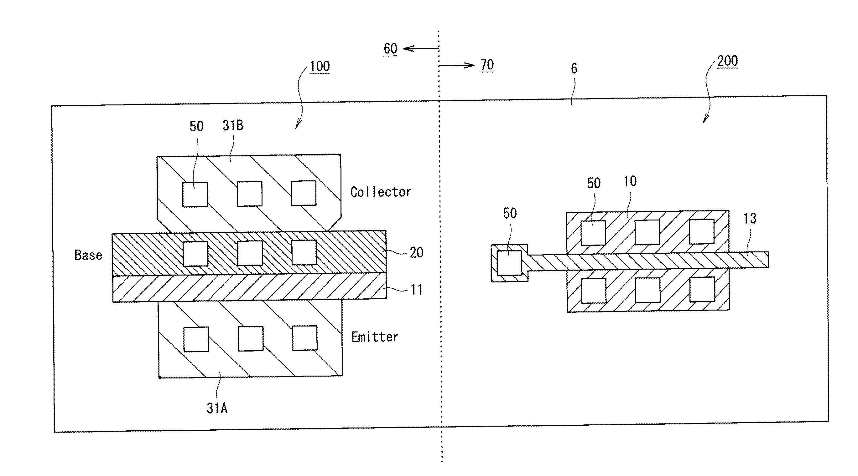
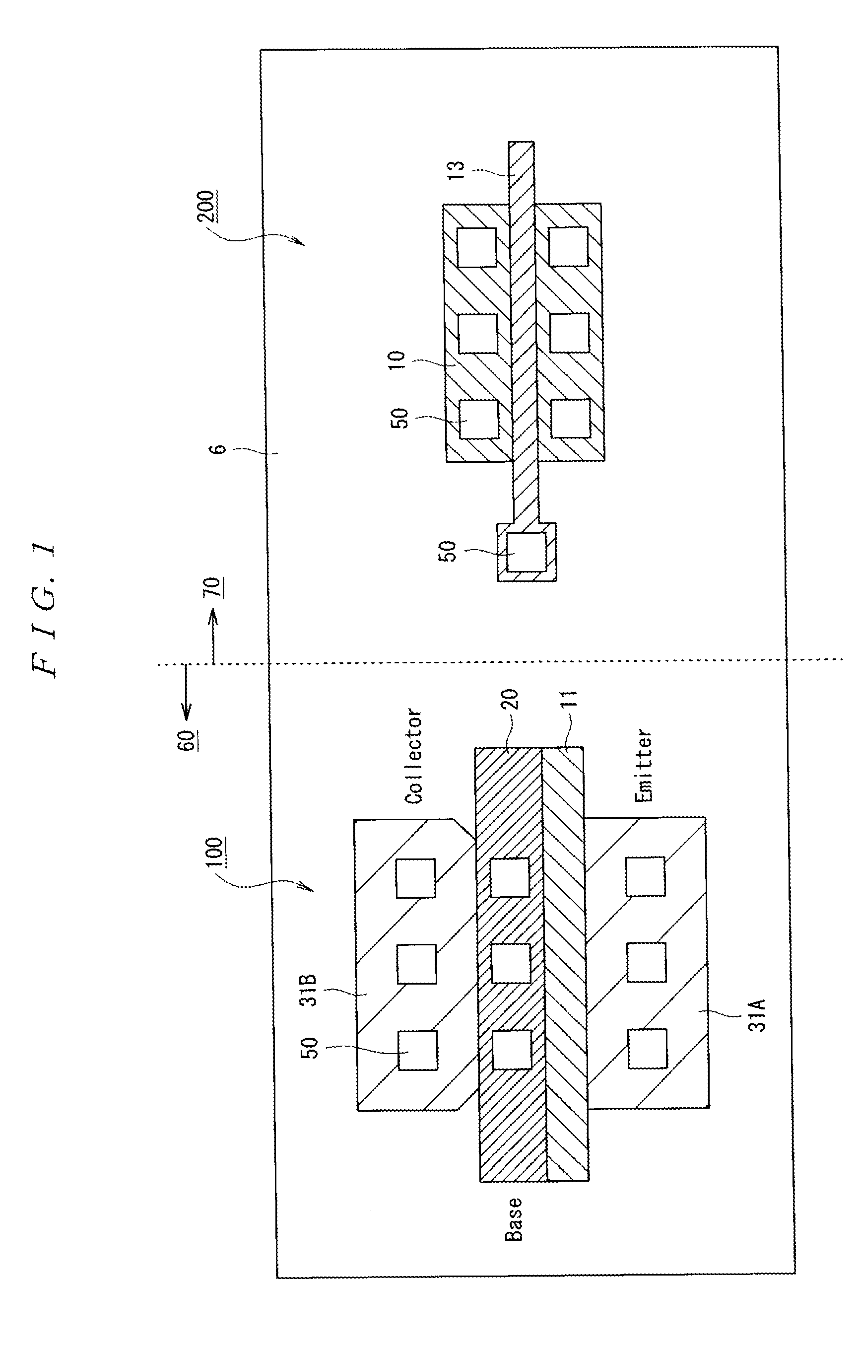
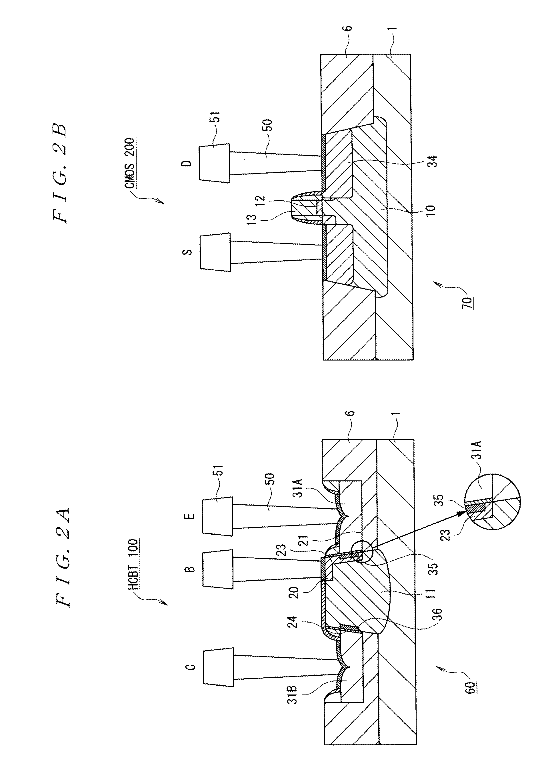
[0129]FIG. 1 is a top view of the semiconductor device according to a first embodiment of the present invention, and is used to explain a state in which a lateral bipolar transistor and a CMOS transistor are hybrid-integrated. The semiconductor device according to the first embodiment is configured by hybrid-integrating an HCBT 100, which is the lateral bipolar transistor, and a CMOS transistor 200 on a device isolating oxide film 6 formed on an Si substrate to serve as a shallow trench isolation. In a region of the device isolating oxide film 6 in which the HCBT 100 is formed is described as an HCBT region 60, an a region the device isolating oxide film 6 in which the CMOS transistor 200 is formed is described as a CMOS region 70.

[0130]As illustrated in the figure, the HCBT 100 includes a collector, a base and an emitter. The collector has a collector electrode 31B and the emitter has an emitter electrode 31A. The base has an extrinsic base layer 20 and an intrinsic base layer 23 o...

second embodiment

[0195]Next, a second embodiment of the present invention will be described. The second embodiment differs from the first embodiment in a method for forming a HCBT collector contact region. That is, in the first embodiment, solid-phase diffusion from polysilicon causes the active region to form the collector diffusion layer, whereas in the second embodiment, the collector diffusion layer is directly formed in an upper portion of the active region without the intervention of polysilicon. Since polysilicon is used only for the emitter diffusion layer, such a configuration of the second embodiment will be referred to as single-polysilicon type HCBT.

[0196]FIG. 30A illustrates a standard mask set used for a single-polysilicon type HCBT. As illustrated in FIG. 30A, an HCBT can be hybrid-integrated together with a CMOS by typically using three additional masks. Integration with a fewer number of masks is also possible. FIG. 30B illustrates masks already available in a CMOS process and also ...

third embodiment

[0251]Furthermore, if the thickness of the emitter polysilicon region decreases in part and a hole is defined therein, an interconnect layer immediately above the hole fails to have adequate contact, as explained in FIG. 31G. However, since the polysilicon 329 is deposited along the contours of the n-hill layer 312 and the device isolating oxide film 320, as illustrated in FIG. 36A, depressions 331 arise on a surface of the polysilicon 329. Since the shape of each of these depressions 331 is traced as the shape of the polysilicon 329 after TMAH-based polysilicon etch back is performed, a hole may be defined in polysilicon 329′ after etch back, as illustrated in FIG. 36B.

[0252]According to the present invention, a polysilicon film called dummy gate polysilicon 706 is formed on a surface of the device isolating oxide film 320, and emitter polysilicon 510 is deposited on top of the dummy gate polysilicon 706. By doing so, the effects of depressions in the polysilicon film 329 are elimi...


PUM


Abstract

A configuration of a lateral transistor suited for the hybrid-integration (BiCMOS) of a high-performance lateral transistor (HCBT) and a CMOS transistor, and a method for manufacturing the lateral transistor are provided. A semiconductor device includes a HCBT 100 and a CMOS transistor 200 hybrid-integrated therein. The HCBT 100 has an open region 21 opened by etching a device isolating oxide film 6 surrounding an n-hill layer 11, an emitter electrode 31A and a collector electrode 31B each of which is formed in the open region 21 and is composed of a polysilicon film having such a thickness as to expose the n-hill layer 11 exposed by etching the device isolating oxide film, and an ultrathin oxide film 24 covering at least a part of the n-hill layer 11. The ultrathin oxide film 24 functions as a protective film for protecting the n-hill layer 11 from being etched when the polysilicon film is etched to form the emitter electrode 31A and the collector electrode 31B.

Description

TECHNICAL FIELD [0001]The present invention relates to a semiconductor device and a method for manufacturing the semiconductor device. More particularly, the invention relates to a semiconductor device having a BiCMOS transistor configuration in which a CMOS transistor and a bipolar transistor are mounted, and to a method for manufacturing the semiconductor device.BACKGROUND ART[0002]Currently, remarkable progress is being made in technologies related to radio communication, and active research and development efforts are being made of small-sized ICs (Integrated Circuit) to be used in mobile phones. As one of ICs to be used mainly for mobile phones, a system-on-chip, in which an RF (Radio Frequency) circuit and a baseband circuit are mounted together on a single chip (hereinafter also referred to as hybrid integration) is now a focus of attention.[0003]High-speed operation is needed for the RF circuit of the system-on-chip, and, miniaturization is also needed for the structure ther...

Claims


Application Information

Patent Timeline
Patent Type & Authority Applications(United States)
IPC IPC(8): H01L27/06H01L21/8249
CPCH01L21/26513H01L21/8249H01L27/0623H01L29/735H01L29/1008H01L29/1045H01L29/6625H01L29/0808H01L21/2257H01L21/26586H01L29/665H01L29/6659H01L21/2658
Inventor SULIGOJ, TOMISLAVKORICIC, MARKOMOCHIZUKI, HIDENORIMORITA, SOICHI
Owner UNIV OF ZAGREB FACULTY OF ELECTRICAL ENG & COMPUTING
Learn More