Bipolar/bicmos semiconductor device

a semiconductor device and bipolar technology, applied in the direction of semiconductor devices, electrical devices, transistors, etc., can solve the problem of insufficiently large maximum oscillation frequency and other problems

Inactive Publication Date: 2002-09-19
RENESAS ELECTRONICS CORP
View PDF0 Cites 16 Cited by
  • Summary
  • Abstract
  • Description
  • Claims
  • Application Information

AI Technical Summary

Problems solved by technology

Accordingly, the conventional bipolar transistors have a problem that

Method used


Image

  • Bipolar/bicmos semiconductor device
  • Bipolar/bicmos semiconductor device
  • Bipolar/bicmos semiconductor device

Examples


first embodiment

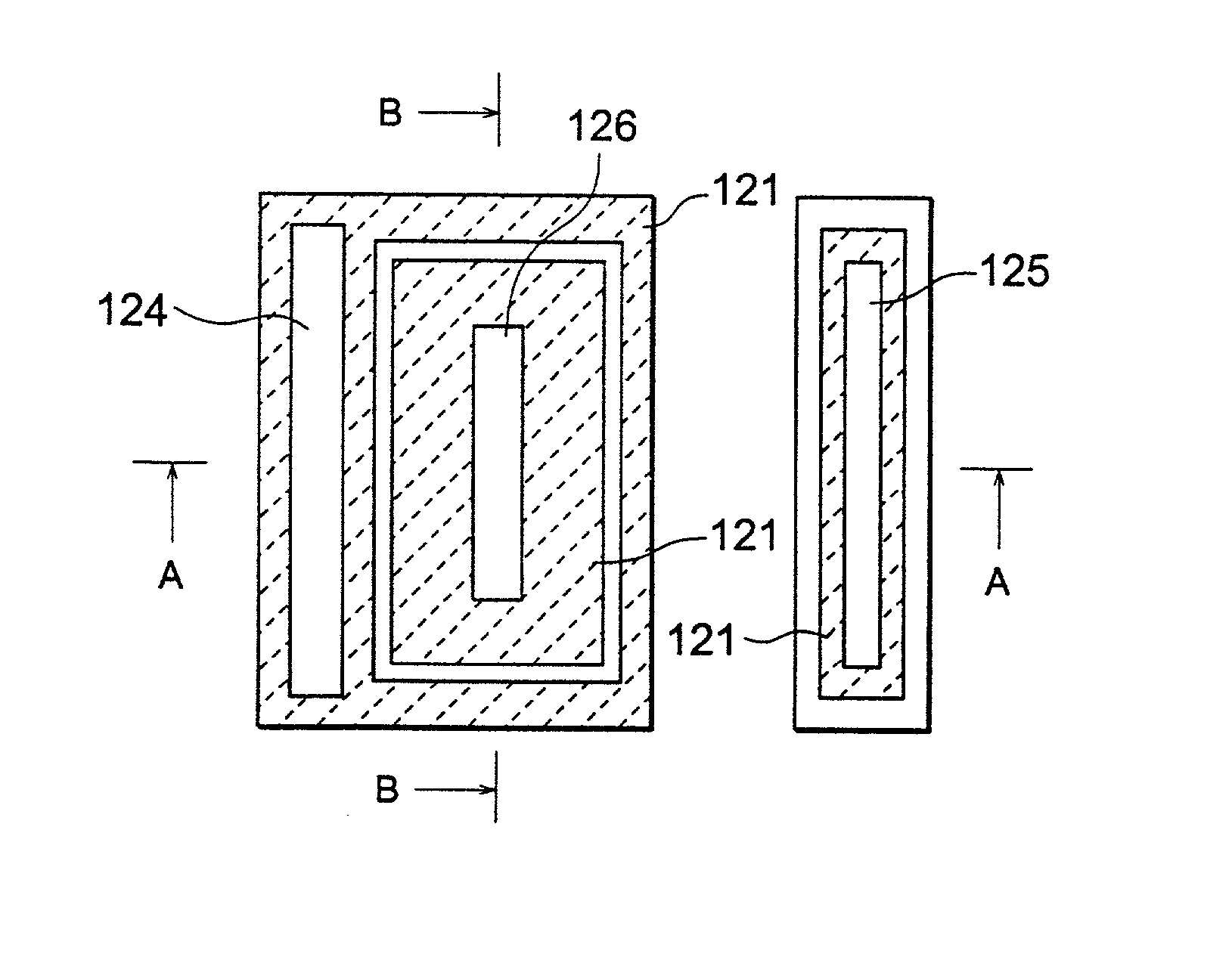
[0066] FIG. 11 is a plan view showing an arrangement of respective layers of a bipolar transistor according to the present invention. FIG. 12 is a sectional view taken along A-A line of FIG. 11. FIG. 13 is a sectional view taken along B-B line of FIG. 11. In the bipolar transistor of the present embodiment, a high-concentration N type buried layer 103 is formed on a P type semiconductor substrate 101. An N type epitaxial area 104 is formed on the substrate 101 to cover the high-concentration N type buried layer. A pedestal collector 112, which is an N type area having an impurity concentration that is in the middle of concentrations of the N type epitaxial area 104 and the high-concentration N type buried layer 103, is formed just under a high-concentration N type diffusion layer 120, which is an emitter region in the N type epitaxial area 104. The high-concentration N type buried layer 103, the N type epitaxial area 104 and the pedestal collector 112 makes the collector area of the...

third embodiment

[0092] The following will describe a third embodiment, referring to FIG. 25, and FIG. 26 taken along C-C line thereof. In many cases, basic blocks of a bipolar transistor generally used in an analogue circuit have a plurality of metal leading-out wirings for its emitter, base and collector in order to improve factors having an influence on its analogue characteristics, for example, its base resistance and high frequency noise (Nf).

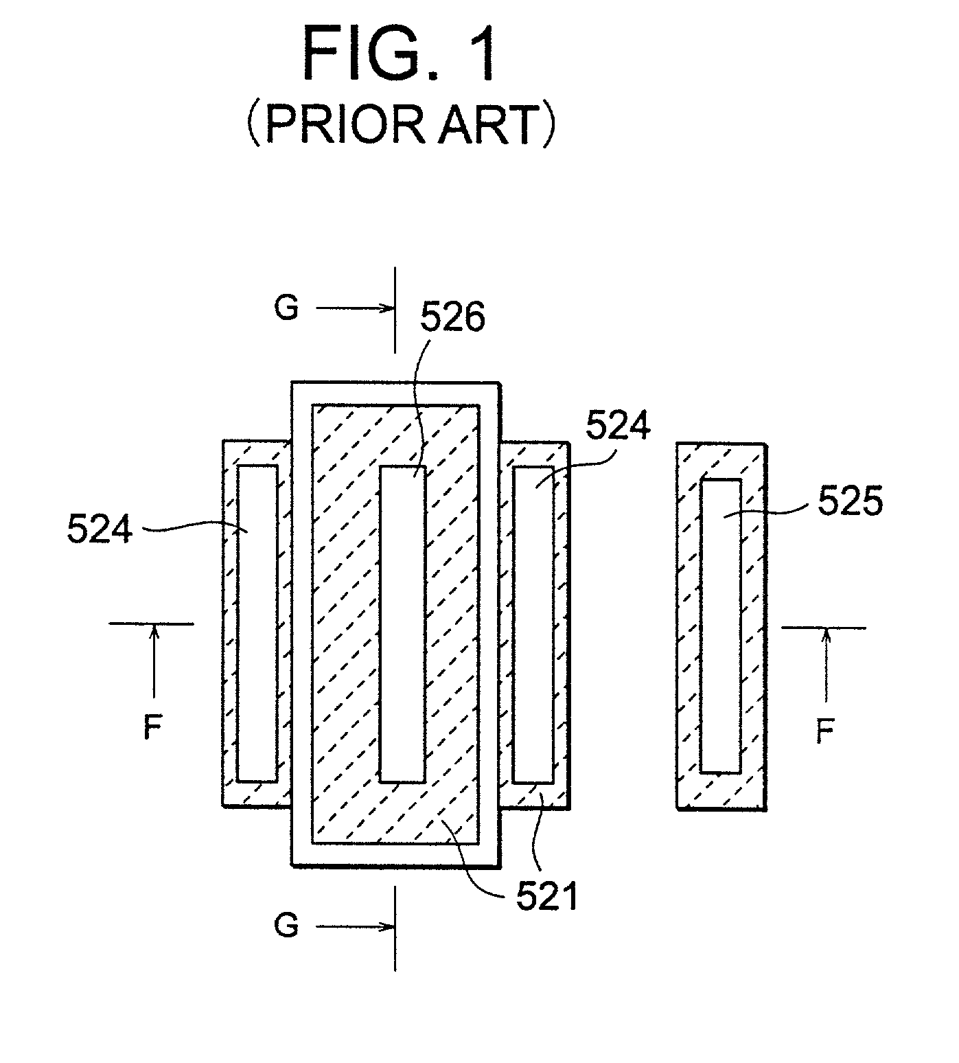
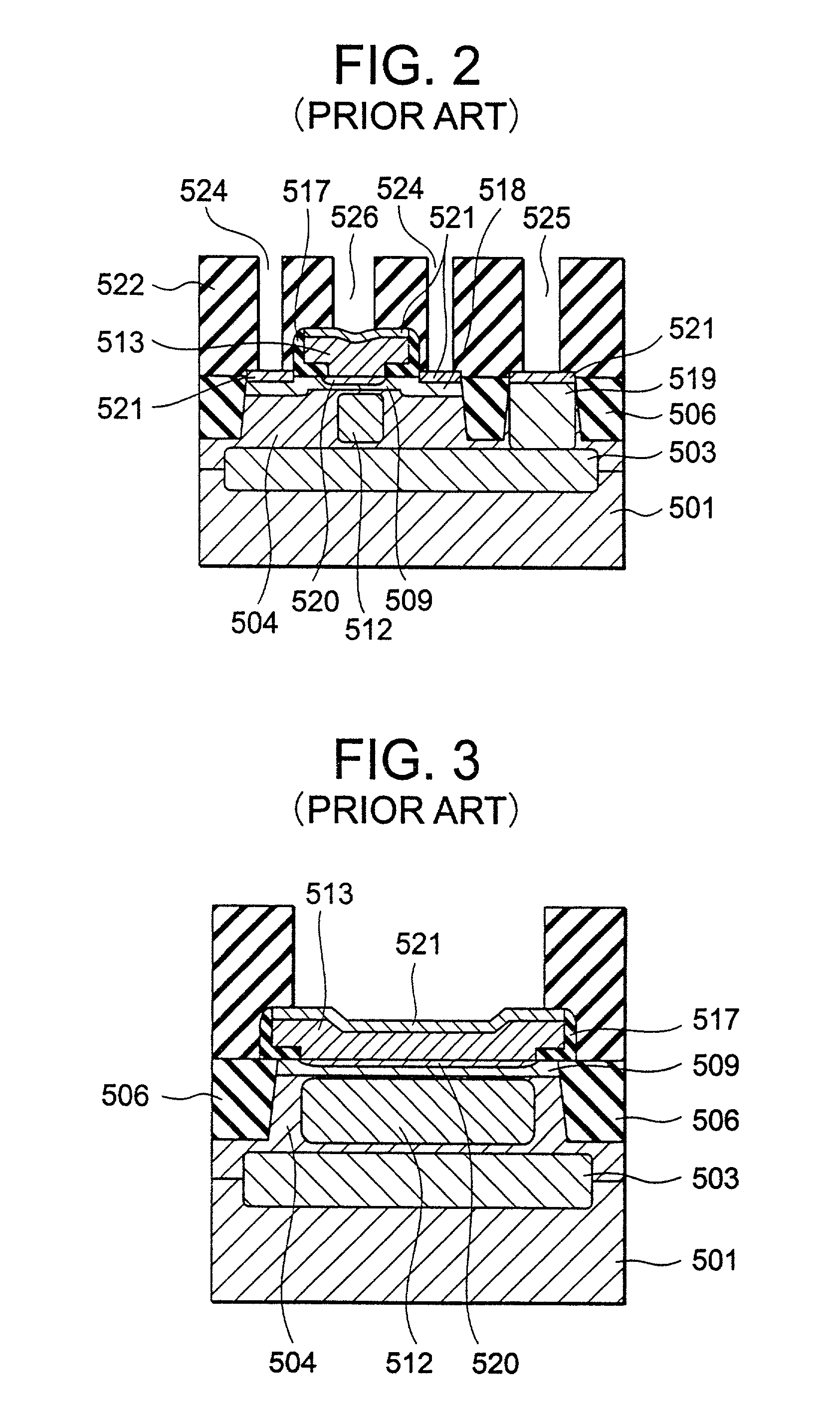
[0093] In order to realize this in the prior art, 7 wirings and 7 contacts are necessary as shown in FIG. 9 and FIG. 10, which is a sectional view taken along E-E line thereof. In FIGS. 9 and 10, a plan view layout in the prior art has contacts for the following from the left side: a collector / a base / an emitter / a base / an emitter / a base / a collector. In FIG. 10, reference numbers 534 and 533 represent wirings for the collector, the base and the emitter, and contact plugs connecting to the wiring 534. The contact plugs are buried in a non-illustrated interlay...


PUM


Abstract

An N type buried layer is buried in a P type silicon substrate. An N type epitaxial layer is formed on this buried layer. A P type intrinsic base region and an extrinsic base region are formed on the surface of the epitaxial layer. An N type emitter region is formed in the intrinsic base region. An emitter electrode is formed to contact the emitter region. A collector plug region is formed in an area separated from the extrinsic base region through a filed insulating film. A cobalt silicide film is formed on the extrinsic base region to surround the emitter electrode. An extrinsic base contact hole is formed at only one side of the emitter electrode. In the semiconductor device, the base resistance Rb and the collector-base capacity Ccb are reduced to make the maximum oscillation frequency fmax sufficiently large.

Description

[0001] 1. Field of the Invention[0002] The present invention relates to a semiconductor device which is useful for the application to a BiCMOS transistor wherein a bipolar transistor and a CMOS transistor are intermixed, and a process for fabricating the same; and in particular to a semiconductor device wherein a bipolar transistor is improved, and a process for fabricating the same.[0003] 2. Description of the Prior Art[0004] Recently, it has been demanded to improve the performance of an analogue / digital intermixing LSI (large scale integrated circuit), wherein an analogue circuit and a digital circuit are mounted inside a single chip, and reduce costs thereof with rapid popularization of a personal handy system (PHS), a portable telephone, a communication terminal for a network, and the like.[0005] In general, a CMOS transistor, which can easily make its consumption electric power small, is used as a digital circuit corresponding to high-speed action in the analog / digital intermi...

Claims


Application Information

Patent Timeline
IPC IPC(8): H01L29/43H01L29/73H01L29/732H01L21/8249H01L21/8222H01L29/417H01L21/8248H01L21/331H01L29/423H01L27/06H01L21/28
CPCH01L29/41708H01L29/7322H01L29/66272H01L29/42304
Inventor SUZUKI, HISAMITSU
Owner RENESAS ELECTRONICS CORP
Why Eureka
Try Eureka