Poly-poly/MOS capacitor having a gate encapsulating first electrode layer

a poly-poly/mos capacitor and gate technology, applied in the field of bicmos, can solve the problems of difficult fabrication of metal-metal capacitors, inferior electrical characteristics of metal-metal capacitors,

Inactive Publication Date: 2003-01-14
GLOBALFOUNDRIES INC
View PDF17 Cites 15 Cited by
  • Summary
  • Abstract
  • Description
  • Claims
  • Application Information

AI Technical Summary

Benefits of technology

Another aspect of the present invention relates to a process of fabricating the above-defined stacked Poly-Poly/MOS capacitor. The process of the present invention can be easily implemented into existing BiCMOS processing schemes so as to provide a BiCMOS device that includes at least the stacked Poly-Poly/MOS capacitor of the present invention therein as one of the device components. Specifically, the method of the present invention comprises the steps of: forming an oxide layer on a surface of a semi...

Problems solved by technology

Despite its high precision, a Poly-Poly capacitor is a compromise between high cost and ideal capacitor characteristics since it is relatively easy to construct, and has electrical characteris...

Method used


Image

  • Poly-poly/MOS capacitor having a gate encapsulating first electrode layer
  • Poly-poly/MOS capacitor having a gate encapsulating first electrode layer
  • Poly-poly/MOS capacitor having a gate encapsulating first electrode layer

Examples


Embodiment Construction

The present invention, which provides a stacked Poly-Poly / MOS capacitor and a method of fabricating the same, will now be described in more detail by referring to the drawings that accompany the present application. It should be noted that in the accompanying drawings like and corresponding elements are referred to by like reference numerals.

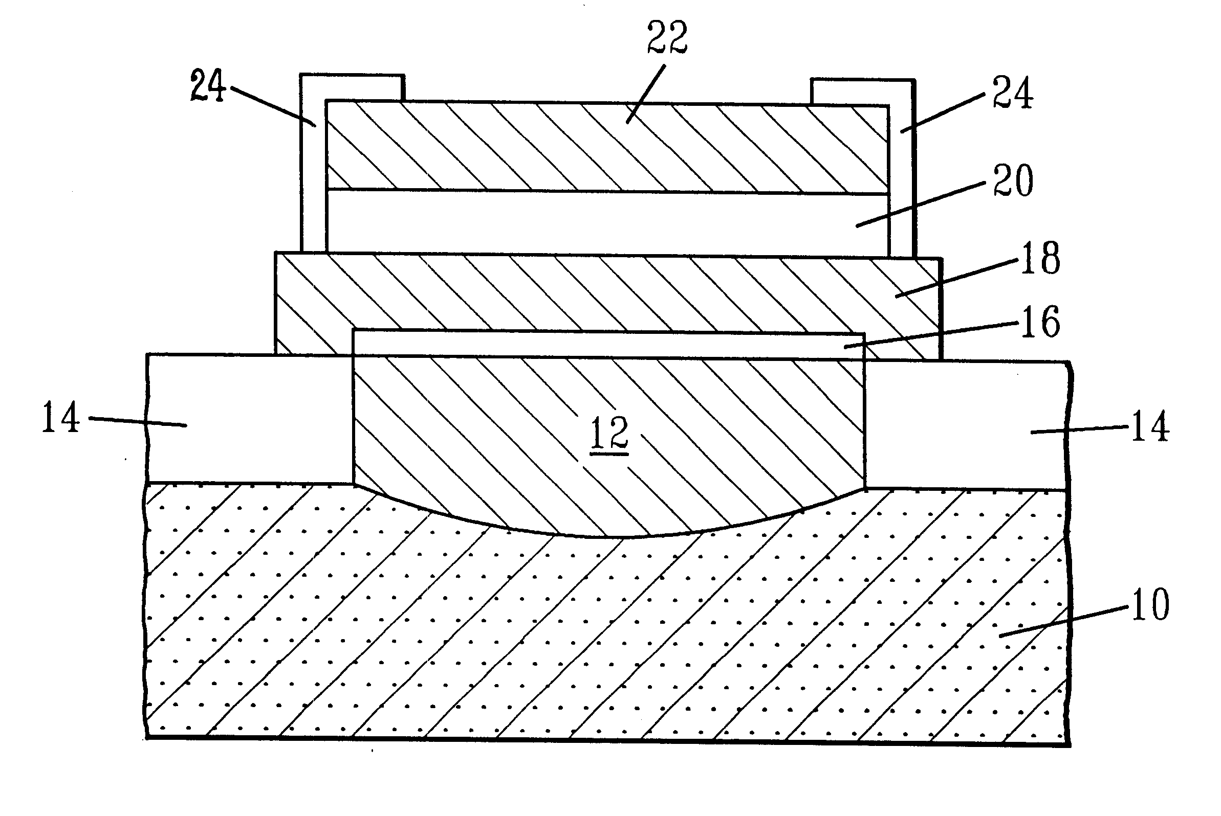
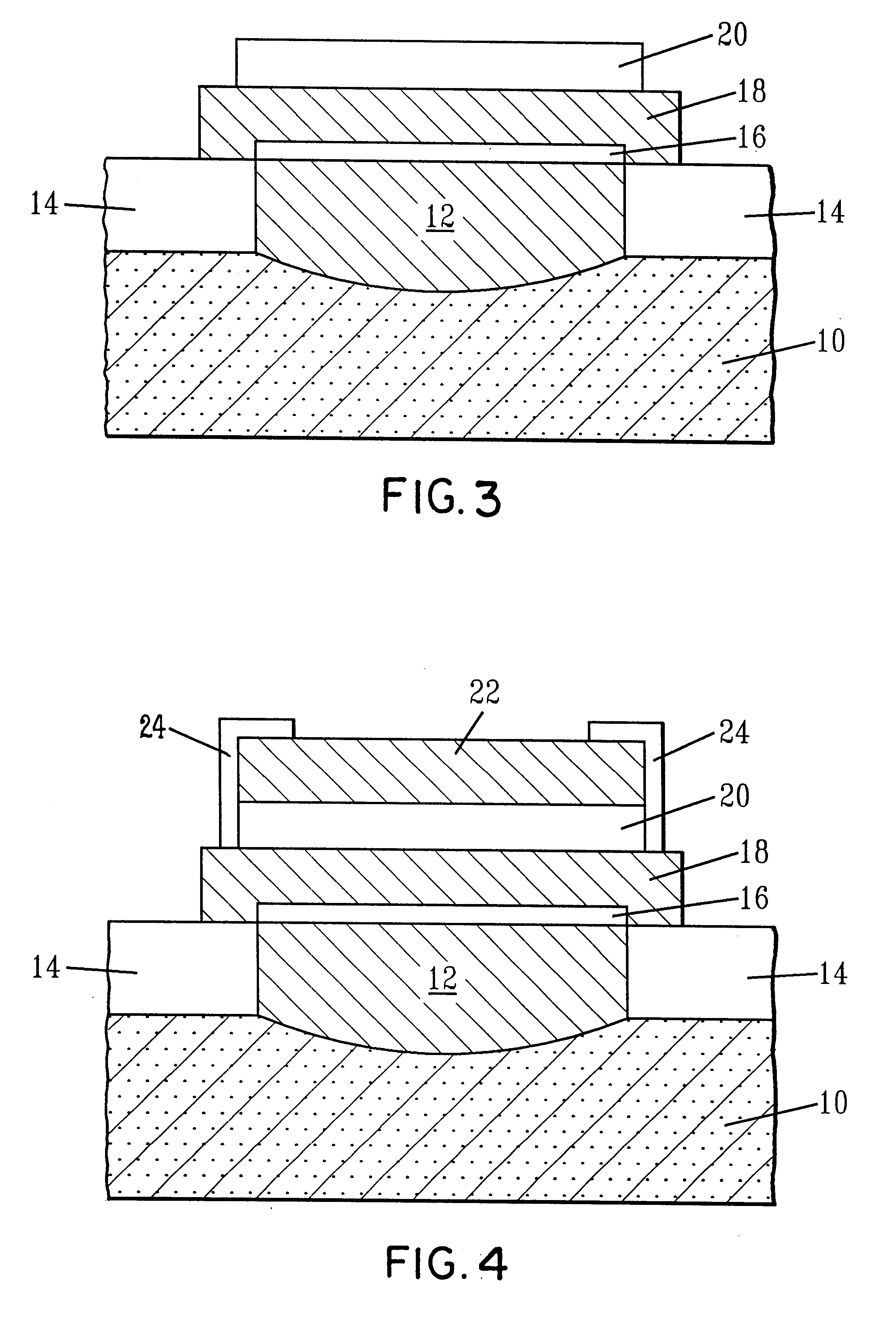
Reference is first made to FIG. 4 which illustrates a basic stacked Poly-Poly / MOS capacitor of the present invention. It is noted that the stacked capacitor shown in the drawing represents one device region of a BiCMOS device. Other device regions including bipolar device regions and CMOS device regions can be formed abutting the stacked Poly-Poly / MOS capacitor shown in FIG. 4. For simplicity, the other device regions of the BiCMOS structure have been omitted.

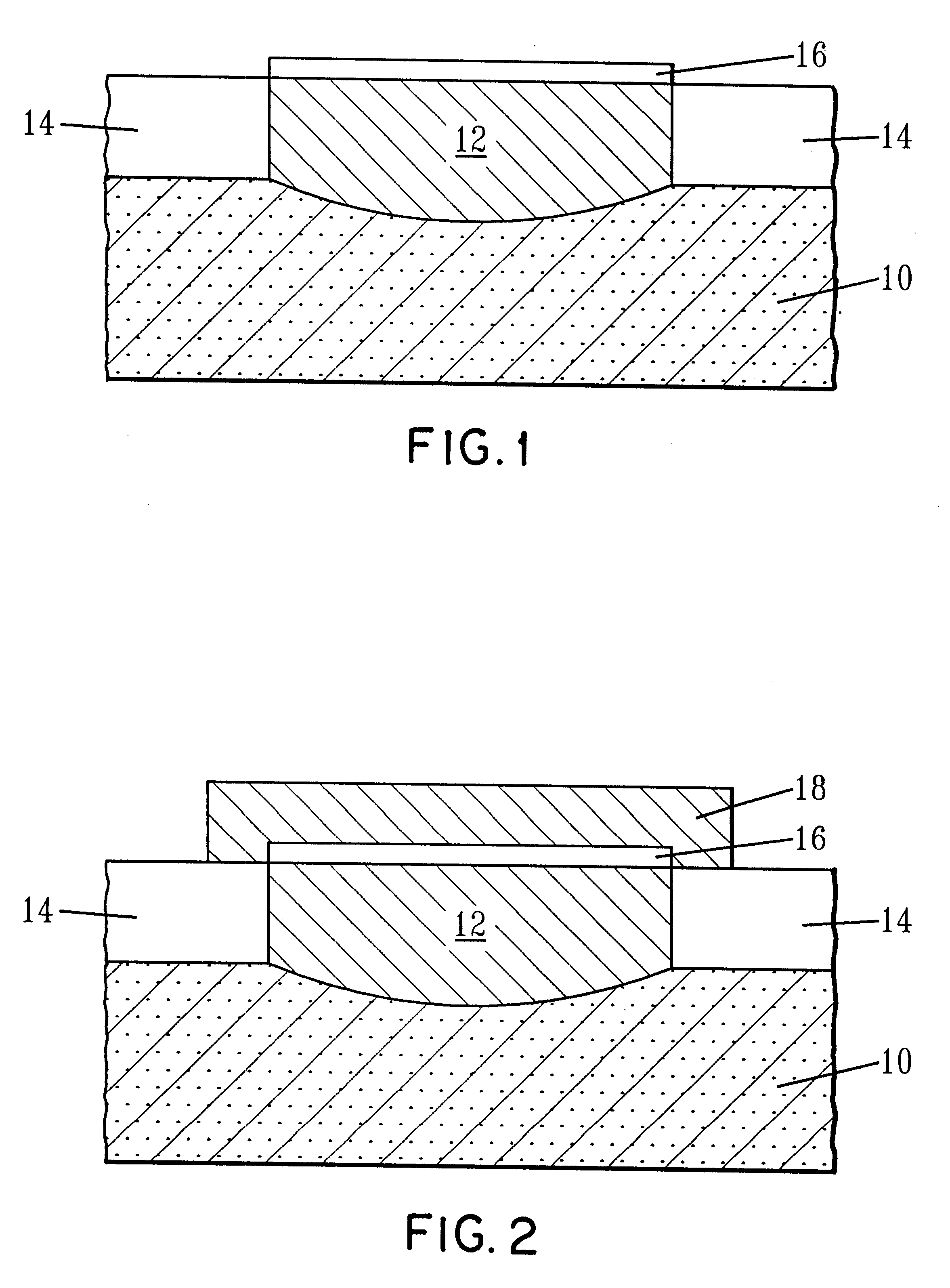
Specifically, the stacked Poly-Poly / MOS capacitor of FIG. 4 comprises a semiconductor substrate 10 that includes trench isolation regions 14 and a region of a first conductivity-type 12 for...


PUM


Abstract

A stacked Poly-Poly/MOS capacitor useful as a component in a BiCMOS device comprising a semiconductor substrate having a region of a first conductivity-type formed in a surface thereof; a gate oxide formed on said semiconductor substrate overlaying said region of first conductivity-type; a first polysilicon layer formed on at least said gate oxide layer, said first polysilicon layer being doped with an N or P-type dopant; a dielectric layer formed on said first polysilicon layer; and a second polysilicon layer formed on said dielectric layer, said second polysilicon layer being doped with the same or different dopant as the first polysilicon layer.

Description

FIELD OF THE INVENTIONThe present invention relates to a BiCMOS, i.e., bipolar and complementary metal oxide semiconductor (CMOS), device, and in particular to a BiCMOS device in which the capacitor component thereof comprises a stacked polysilicon-polysilicon (Poly-Poly) / metal oxide semiconductor (MOS) capacitor. The present invention also provides a method of fabricating a stacked Poly-Poly / MOS capacitor in which the processing steps thereof can be integrated into various BiCMOS integration schemes.BACKGROUND OF THE INVENTIONIn the field of semiconductor device manufacturing, CMOS (complementary metal oxide semiconductor) and BiCMOS (bipolar device and complementary metal oxide semiconductor) technologies have been widely used for integrating highly complex analog-digital subsystems onto a single chip. In such subsystems, high precision capacitors are typically required.Several types of capacitors are available including Poly-Poly capacitors, MOS capacitors (also referred to in th...

Claims


Application Information

Patent Timeline
IPC IPC(8): H01L29/66H01L21/02H01L29/94H01L27/04H01L21/822H01L21/8249H01L27/06
CPCH01L29/94H01L28/40H01L27/0805H01L27/06
Inventor COOLBAUGH, DOUGLAS D.DUNN, JAMES STUARTST. ONGE, STEPHEN ARTHUR
Owner GLOBALFOUNDRIES INC
Why Eureka
Try Eureka