Laser diode device

a diode device and laser technology, applied in the direction of laser details, laser cooling arrangements, semiconductor lasers, etc., can solve the problems of difficult to reduce the resistance of the cladding layer, increase the light loss, etc., and achieve the effect of increasing the surface area of the contact layer and low voltage driv

Inactive Publication Date: 2011-06-28
SONY CORP
View PDF3 Cites 1 Cited by
  • Summary
  • Abstract
  • Description
  • Claims
  • Application Information

AI Technical Summary

Benefits of technology

[0008]In the laser diode device, since the concavo-convex structure is formed on the face on the electrode side of the contact layer, the surface area of the contact layer is increased. Further, since the electrode is contacted with the contact layer at contact points of the top face, the side face, and the bottom face of the concavo-convex structure, the contact area between the electrode and the contact layer is increased. Accordingly, low voltage drive is able to be realized.

Problems solved by technology

When the film thickness of the cladding layer is decreased, it causes increase of light loss.
Further, it is difficult to decrease resistance of the cladding layer, since concentration of p-type carrier is hardly increased particularly in the case of nitride semiconductor.

Method used


Image

  • Laser diode device
  • Laser diode device
  • Laser diode device

Examples


Embodiment Construction

f manufacturing the laser diode device illustrated in FIG. 1 in the order of steps;

[0020]FIG. 10 is a cross sectional view illustrating a step following FIG. 9;

[0021]FIG. 11 is a cross sectional view illustrating a step following FIG. 10;

[0022]FIG. 12 is a cross sectional view illustrating a step following FIG. 11; and

[0023]FIG. 13 is a cross sectional view illustrating another modified example of the laser diode device illustrated in FIG. 1.

DETAILED DESCRIPTION OF THE PREFERRED EMBODIMENT

[0024]An embodiment of the invention will be hereinafter described in detail with reference to the drawings.

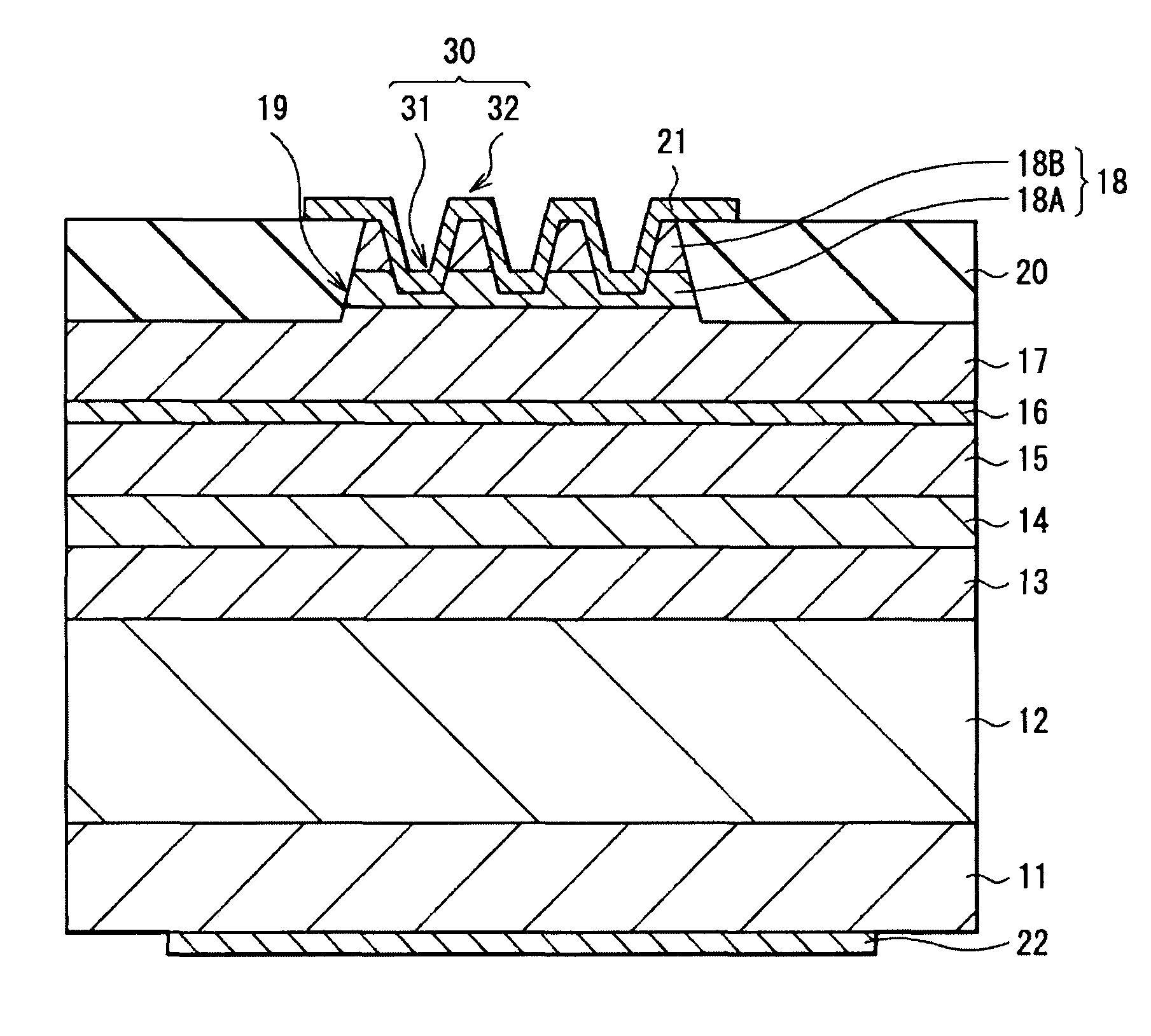
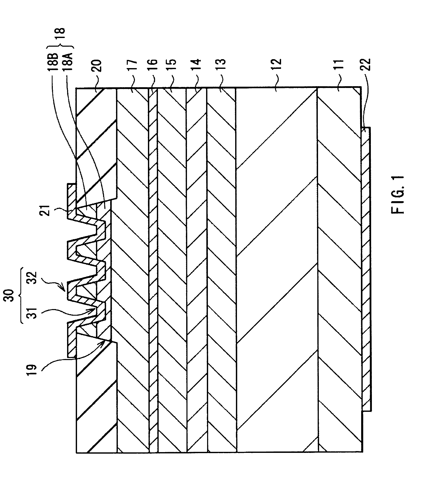
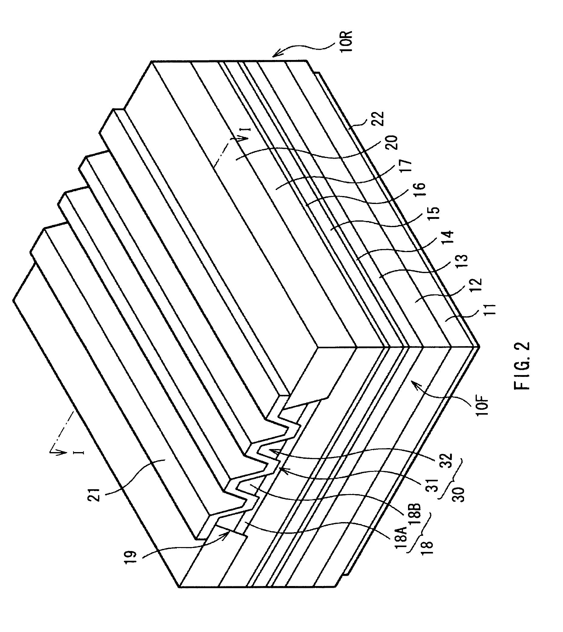
[0025]FIG. 1 and FIG. 2 illustrate a structure of a laser diode device according to an embodiment of the invention. The laser diode device is a blue / blue-violet laser diode device having an oscillation wavelength of about 500 nm or less, for example, around 400 nm that is used for, for example, a BD recording / reproducing laser of a personal computer, a home-use game machine and the like. For ...


PUM


Abstract

A laser diode device with which a low voltage is realized is provided. The laser diode device includes: a substrate; a semiconductor laminated structure including a first conductive cladding layer, an active layer, and a second conductive cladding layer on one face side of the substrate and having a contact layer as the uppermost layer, in which a protrusion is formed in the contact layer and the second conductive cladding layer; and an electrode provided on the contact layer. The contact layer has a concavo-convex structure on a face on the electrode side, and the electrode is contacted with the contact layer at contact points of a top face, a side face, and a bottom face of the concavo-convex structure.

Description

BACKGROUND OF THE INVENTION[0001]1. Field of the Invention[0002]The present invention relates to a laser diode device particularly suitable for a ridge type laser diode.[0003]2. Description of the Related Art[0004]In the past, the ridge type laser diode in which a current confinement is made by forming a strip-shaped protrusion (ridge) in a p-side contact layer and a p-type cladding layer correspondingly to a current injection region of an active layer has been known (for example, see Japanese Unexamined Patent Application Publication No. 2007-300016).SUMMARY OF THE INVENTION[0005]In such an existing ridge-type laser diode, in order to realize a low voltage, it is necessary to increase the width of the protrusion (stripe width), decrease a film thickness of a cladding layer, or decrease resistance of the cladding layer. However, when the width of the protrusion is increased, kink level is lowered. When the film thickness of the cladding layer is decreased, it causes increase of ligh...

Claims


Application Information

Patent Timeline
Patent Type & Authority Patents(United States)
IPC IPC(8): H01S5/00
CPCH01S5/0421H01S5/028H01S5/0425H01S5/327H01S5/22H01S5/2215H01S5/32341H01S5/2009H01S5/04254
Inventor OBATA, TOSHIYUKI
Owner SONY CORP
Why Eureka
Try Eureka