Computer-implemented methods for determining if actual defects are potentially systematic defects or potentially random defects

a technology of computer implementation and actual defects, applied in error detection/correction, program control, instruments, etc., can solve problems such as the need to detect defects of decreasing size, the operation of semiconductor manufacturing processes closer to the limitations of process performance capability, and the impact of small defects on the electrical parameters of devices

Active Publication Date: 2011-07-05
KLA CORP
View PDF385 Cites 10 Cited by
  • Summary
  • Abstract
  • Description
  • Claims
  • Application Information

AI Technical Summary

Benefits of technology

[0028]Each of the steps of the method described above may be further performed as described herein. In addition, the embodiment of the method described above may include any other step(s) of any other method(s) described herein. Furthermore, the embodiment of the method described above may be performed by any of the systems described herein.
[0030]FIG. 1 is a die map illustrating one example of die stacking results showing actual defects detected on a wafer;

Problems solved by technology

However, as the dimensions of semiconductor devices decrease, inspection becomes even more important to the successful manufacture of acceptable semiconductor devices because smaller defects can cause the devices to fail.
For instance, as the dimensions of semiconductor devices decrease, detection of defects of decreasing size has become necessary since even relatively small defects may cause unwanted aberrations in the semiconductor devices.
As design rules shrink, however, semiconductor manufacturing processes may be operating closer to the limitations on the performance capability of the processes.
In addition, smaller defects can have an impact on the electrical parameters of the device as the design rules shrink, which drives more sensitive inspections.
Therefore, as design rules shrink, the population of potentially yield relevant defects detected by inspection grows dramatically.
As a result, more and more defects may be detected on the wafers, and correcting the processes to eliminate all of the defects may be difficult and expensive.
Furthermore, at smaller design rules, process induced failures may, in some cases, tend to be systematic.
That is, process induced failures tend to fail at predetermined design patterns often repeated many times within the design.
In addition, although defects are generally related to process and design interaction, process induced failures are defects that are created from the artifacts of process variation not necessarily due to weak design and process variations.
However, such methods have a number of disadvantages.
In addition, random defect groups are known to often have higher defect counts than defect counts of systematic defect groups.
As such, these previously used methods may produce incorrect results by identifying groups of random defects as potential systematic defects.
In addition, the Pareto chart cut-line based methods may not be effective for determining which defect bins include potentially systematic defects since, if it is assumed that all defects on a given wafer are random defects (i.e., a 0% systematic assumption), then the defect counts shown in a Pareto chart illustrating the results of design based grouping may report only the relative area of different circuit structures on the wafer.

Method used


Image

  • Computer-implemented methods for determining if actual defects are potentially systematic defects or potentially random defects
  • Computer-implemented methods for determining if actual defects are potentially systematic defects or potentially random defects
  • Computer-implemented methods for determining if actual defects are potentially systematic defects or potentially random defects

Examples


Embodiment Construction

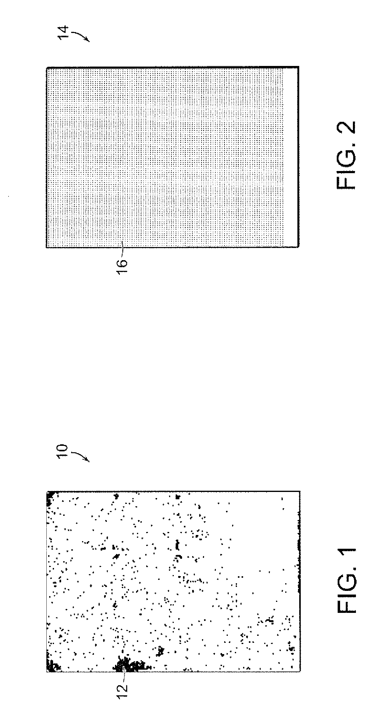
[0038]As used herein, the term “actual defects” refers to actual defects detected on a wafer. Therefore, the term “actual defects” does not refer to actual defects that may be present on a wafer but have not been detected on the wafer.

[0039]As used herein, the term “wafer” generally refers to substrates formed of a semiconductor or non-semiconductor material. Examples of such a semiconductor or non-semiconductor material include, but are not limited to, monocrystalline silicon, gallium arsenide, and indium phosphide. Such substrates may be commonly found and / or processed in semiconductor fabrication facilities.

[0040]A wafer may include one or more layers formed upon a substrate. For example, such layers may include, but are not limited to, a resist, a dielectric material, a conductive material, and a semiconductive material. Many different types of such layers are known in the art, and the term wafer as used herein is intended to encompass a wafer including all types of such layers....


PUM


Abstract

Various computer-implemented methods for determining if actual defects are potentially systematic defects or potentially random defects are provided. One computer-implemented method for determining if actual defects are potentially systematic defects or potentially random defects includes comparing a number of actual defects in a group to a number of randomly generated defects in a group. The actual defects are detected on a wafer. A portion of a design on the wafer proximate a location of each of the actual defects in the group and each of the randomly generated defects in the group is substantially the same. The method also includes determining if the actual defects in the group are potentially systematic defects or potentially random defects based on results of the comparing step.

Description

PRIORITY CLAIM[0001]This application claims priority to U.S. Provisional Application Nos. 60 / 956,823 entitled “Computer-Implemented Methods for Determining if Actual Defects are Systematic Defects or Random Defects,” filed Aug. 20, 2007, which is incorporated by reference as if fully set forth herein.BACKGROUND OF THE INVENTION[0002]1. Field of the Invention[0003]The present invention generally relates to computer-implemented methods for determining if actual defects are potentially systematic defects or potentially random defects. Certain embodiments relate to determining if actual defects are potentially systematic defects or potentially random defects by comparing actual defects grouped by design to randomly generated defects grouped by design.[0004]2. Description of the Related Art[0005]The following description and examples are not admitted to be prior art by virtue of their inclusion in this section.[0006]An integrated circuit (IC) design may be developed using a method or sys...

Claims


Application Information

Patent Timeline
Patent Type & Authority Patents(United States)
IPC IPC(8): G06F17/50
CPCG01R31/318314G06F17/5081G01R31/318371G06F30/398
Inventor FLORENCE, GLENNPARK, ALLENROSE, PETER
Owner KLA CORP
Why Eureka
Try Eureka