

Optical modulator
a modulator and optical technology, applied in the field of optical modulators, can solve the problems of deteriorating receiver sensitivity and chromatic dispersion tolerance, inter-symbol interference between transmitting waveforms, and difficult to obtain ideal rectangular waveforms
- Summary
- Abstract
- Description
- Claims
- Application Information
AI Technical Summary
Benefits of technology
Problems solved by technology
Method used
Image

Examples
first embodiment
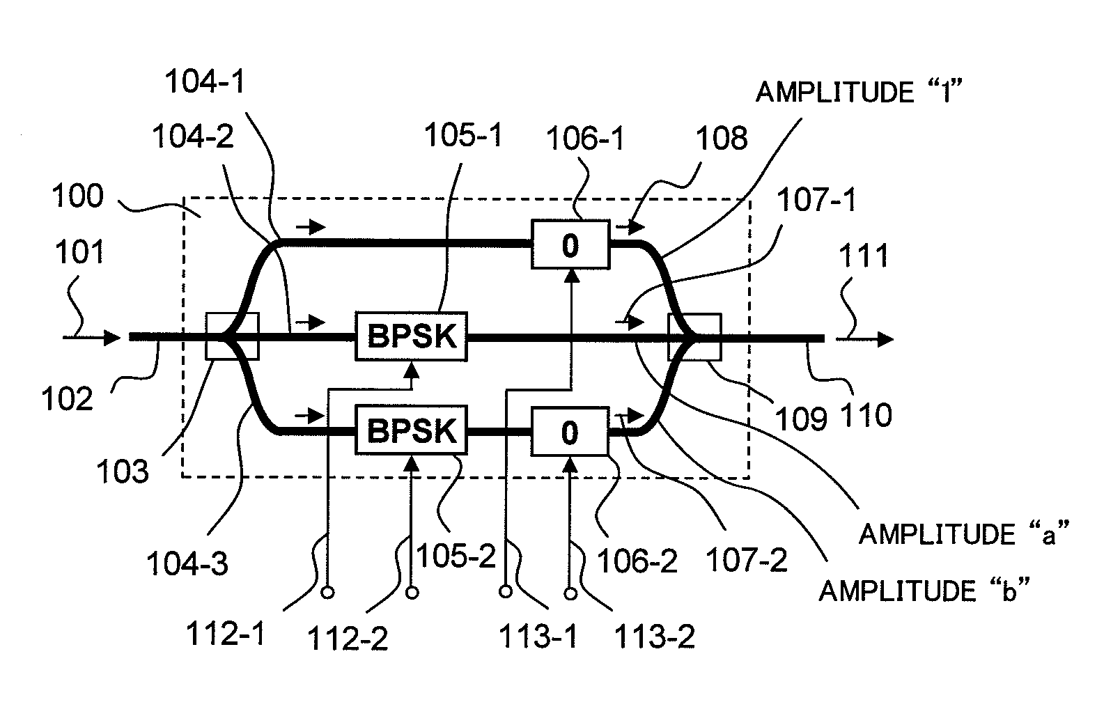
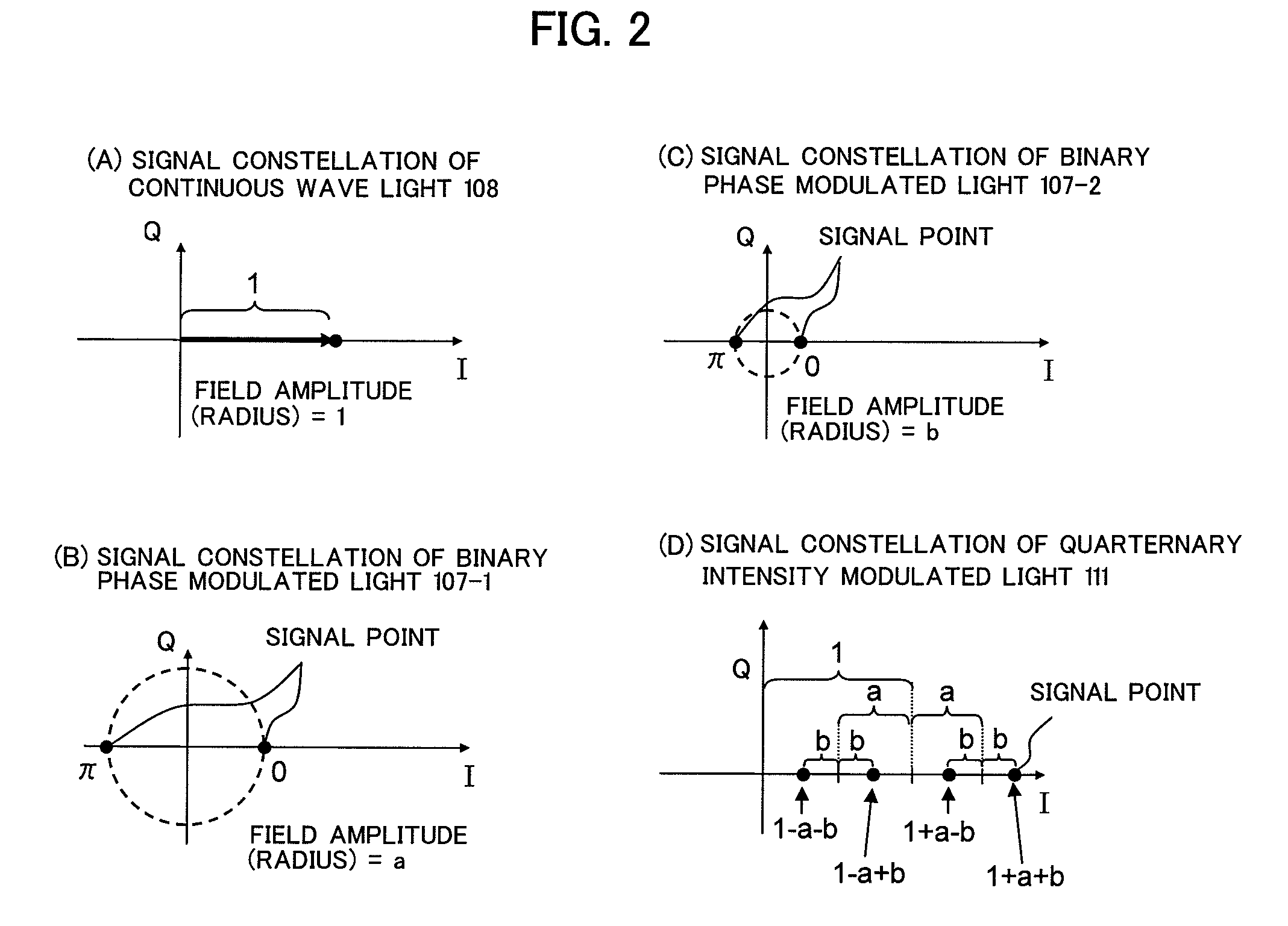
[0059]FIG. 1 shows a configuration of a quaternary optical amplitude modulator 100 as the first embodiment of the present invention;
[0060]Input light 101 supplied from an input optical path 102 is split into the first optical path 104-1, the second optical path 104-2, and the third optical path 104-3 by an optical splitter 103. Among these optical paths, in the second optical paths 104-2 and the third optical paths 104-3, single drive MZ type binary optical phase modulators 105-1 and 105-2 are arranged, respectively, and in the first optical path 104-1 and the third optical path 104-3, optical phase adjusters 106-1 and 106-2 are arranged, respectively.
[0061]To the modulated signal input terminals 112-1 and 112-2 of the binary optical phase modulators 105-1 and 105-2, individual binary electric digital signals are supplied, respectively. These electrical signals have the same bit rate with each other and respective signal delay amount are adjusted so that the bit timings are matched ...
second embodiment
[0085]FIG. 13 shows a quaternary optical amplitude modulator 100A provided with an automatic phase adjusting function as the second embodiment of the present invention.
[0086]When the length of each optical path connected to the optical coupler 109 varies, for example, due to environment temperature change or aging, the magnitude of the eye-opening in the waveform of the optical multilevel intensity modulation output from the optical coupler 109 changes and the transmission characteristics are degraded. If the eye-opening changes largely, there is a possibility that the logic values of the digital signals are inverted and the signal transmission becomes impossible. In this case, there is possibility that each signal point also changes in a phase direction so as to cause transmission deterioration by the chirp of the waveform or deterioration in the phase modulation results largely.
[0087]In the second embodiment, in order to prevent such phenomenon, a portion of output light 111 from ...
third embodiment
[0101]FIG. 15 shows a configuration example of an 8-level optical amplitude-and-phase modulator 200 (2-level in amplitude and 4-level in phase) as the third embodiment of the present invention. In the embodiment, a binary optical amplitude modulator 153 which is a basic mode of the present invention is used.
[0102]A continuous wave light 151 output from a semiconductor laser light source 150 is input to a known quadrature quaternary optical phase modulator (QPSK) 133 and converted into quadrature quaternary phase modulated light 152-1. The quadrature quaternary phase modulated light 152-1 is input to a binary optical amplitude modulator 153, whereby subjected to chirp-less binary amplitude modulation. In the binary optical amplitude modulator 153, the input quadrature quaternary optical phase modulated light 152-1 is split into the first optical path 104-1 and the second optical path 104-2. The input light of the first optical path 104-1 is input to the optical coupler 109 in the sta...
PUM
| Property | Measurement | Unit |
|---|---|---|
| voltage amplitude | aaaaa | aaaaa |
| width | aaaaa | aaaaa |
| phase angles | aaaaa | aaaaa |
Abstract
Description
Claims
Application Information