Plasma display panel and drive method therefor

a technology of plasma display panel and drive method, which is applied in the manufacture of electric discharge tubes/lamps, instruments, electrode systems, etc., can solve the problems of weak discharge, low image contrast, and inability to offer dark images in high quality, and achieve enhanced dark contrast, weak reset discharge, and enhanced dark contrast

Inactive Publication Date: 2011-08-02
PANASONIC CORP
View PDF25 Cites 4 Cited by
  • Summary
  • Abstract
  • Description
  • Claims
  • Application Information

AI Technical Summary

Benefits of technology

[0020]Besides, in a case where the opposed discharges between the row electrodes on one side and the column electrodes are reset discharges for initializing all the unit light emission regions at the drive of the PDP, these opposed discharges are performed at substantially the central parts of the unit light emission regions spaced from that substrate of the pair of substrates which forms the panel face of the PDP. Therefore, light emissions based on the reset discharges as are recognized at the panel face become less than in a case where the reset discharges are performed by the surface discharges between the row electrodes at positions near the panel face. Accordingly, a dark contrast is prevented from lowering due to the light emissions which are based on the reset discharges and which have no relation to the gradation display of an image, and enhancement in the dark contrast of the PDP can be attained.
[0046]According to such a drive, at the reset discharges, cations within the discharge gas collide against the secondary electron emission material in advancing toward the side of the column electrodes, and they emit secondary electrons into the discharge space. The discharge initiation voltage of the pixel cells becomes low owing to a priming action based on such secondary electrons, and comparatively weak reset discharges can be induced. Consequently, owing to the weak reset discharges, a light emission intensity involved in the discharges lowers, so that a display in which a dark contrast is enhanced can be presented. Further, the reset discharges are induced between the row electrodes on one side, formed on the side of the front transparent substrate and the column electrodes formed on the side of the rear substrate. Therefore, discharge light which is externally emitted from the side of the front transparent substrate becomes less than in a case where the reset discharges are induced between the row electrodes both of which are formed on the side of the front transparent substrate. Accordingly, further enhancement in the dark contrast can be attained.

Problems solved by technology

Therefore, the PDPs have had the problem that the light emissions induced by the discharges lower the contrast of the image.
According to such a PDP, a priming effect after a discharge continues for a comparatively long time, and hence, a weak discharge can be caused stably.
Even with such a drive method, however, the so-called “dark contrast” in the case of displaying a dark image cannot be satisfactorily heightened, and this has posed the problem that the dark image cannot be offered in a state of high quality.

Method used


Image

  • Plasma display panel and drive method therefor
  • Plasma display panel and drive method therefor
  • Plasma display panel and drive method therefor

Examples


second embodiment

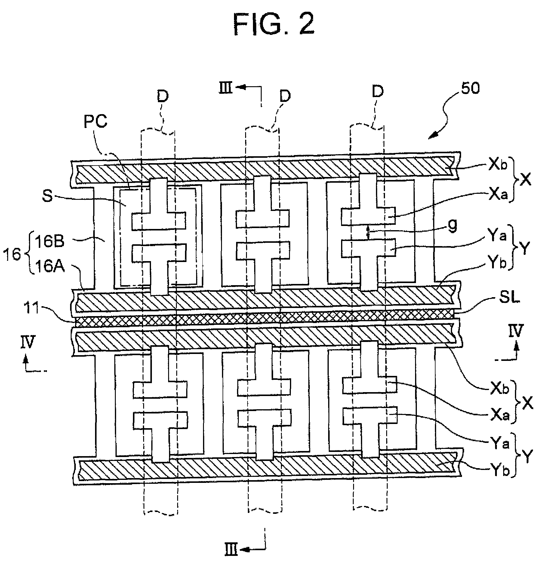
[0164]FIG. 25 is a sectional view showing a PDP according to this invention.

[0165]The fluorophor layer of the PDP of the first embodiment described before is formed by mixing the fluorescent materials and the MgO crystals which are the secondary electron emission material. In contrast, the PDP in the second embodiment is such that a fluorophor layer 17 has a configuration in which an MgO crystal layer 17B that is formed of MgO crystals being a secondary electron emission material is stacked on a fluorescent material layer 17A that is formed of a fluorescent material, and in which the MgO crystal layer 17B is exposed to a discharge cell C.

[0166]The MgO crystal layer 17B may be formed so as to spread the MgO crystals all over the fluorescent material layer 17A. Alternatively, a thin film based on the MgO crystals may well be formed so as to be stacked on the fluorescent material layer 17A.

[0167]In a case where CL emission MgO crystals are employed and contained as the secondary electr...

first embodiment

[0169]The PDP is driven by a method similar to that in the case of the

[0170]More specifically, a reset discharge proceeds in such a way that the row electrode reset pulse in the aspect as shown in FIG. 17 or 23 is impressed on row electrodes Y, whereby opposed discharges based on a cathode column electrode discharge are generated between the row electrodes Y and column electrodes D.

[0171]Thus, as in the case of the first embodiment, the effect of enhancing the dark contrast of the PDP is demonstrated by the opposed discharges of the reset discharge, and the effect of lowering the discharge initiation voltage of an address discharge to succeed to the reset discharge is demonstrated by secondary electrons which are emitted from the MgO crystal layer 17B into the discharge cells C by the reset discharge.

[0172]Besides, in the case where the MgO crystal layer 17B is formed containing the CL emission MgO crystals, the dark contrast can be further enhanced by the shortening of a discharge ...


PUM


Abstract

A plasma display panel and a drive method therefor, which can enhance a representation capability when displaying a dark image. The plasma display panel includes fluorophor layers containing magnesium oxide. The drive method includes a reset step to initialize all the pixel cells into states of one of a light-up mode and a light-off mode, and an address step in which the pixel cells are caused to perform address discharges selectively in accordance with pixel data, which are successively executed in each of a head subfield and a second subfield within a one-field display period. In reset step, a voltage that sets row electrodes on one side, in the row electrode pairs as an anode and sets the column electrodes set as a cathode is applied between the row electrodes on the one side and the column electrodes.

Description

BACKGROUND OF THE INVENTION[0001]1. Field of the Invention[0002]This invention relates to the configuration of a plasma display panel and a drive method for a plasma display panel.[0003]2. Description of the Related Art[0004]Nowadays, as thin-screen display devices, plasma display panels (hereinbelow, abbreviated to the “PDPs”) of AC type (AC discharge type) have been put into commercial production. In the PDP, two substrates, namely, a front transparent substrate and a rear substrate, are arranged in opposition through a predetermined spacing. A plurality of row electrode pairs in which row electrodes forming the respective pairs extend in the lateral direction of a screen are formed on that inner surface of the front transparent substrate (a surface opposing to the rear substrate) which is a display surface. Further, a dielectric layer which covers the respective row electrode pairs are formed on such an inner surface of the front transparent substrate. On the other hand, a plural...

Claims


Application Information

Patent Timeline
Patent Type & Authority Patents(United States)
IPC IPC(8): G09G3/28G09G3/288G09G3/292G09G3/298H01J17/49
CPCG09G3/2927G09G3/2983H01J1/32H01J9/221H01J11/12H01J11/40H01J11/42G09G2310/066G09G2320/0238G09G3/291G09G3/296
Inventor ITAKURA, SHUNSUKEHIROTA, ATSUSHILIN, HAITOKUNAGA, TSUTOMU
Owner PANASONIC CORP
Why Eureka
Try Eureka