Supercharge Your Innovation With Domain-Expert AI Agents!

Nonvolatile semiconductor memory and method for testing the same

a non-volatile semiconductor and memory technology, applied in information storage, static storage, digital storage, etc., can solve the problems of data in the affected unselected cells to be rewritten, the supply voltage cannot be easily changed, and the inability to control the supply voltage to be supplied to the chip, so as to achieve the effect of easy change of the drive voltag

Active Publication Date: 2011-08-02
RENESAS ELECTRONICS CORP
View PDF5 Cites 7 Cited by
  • Summary
  • Abstract
  • Description
  • Claims
  • Application Information

AI Technical Summary

Benefits of technology

The present invention provides a solution for testing nonvolatile semiconductor memory without changing the supply voltage. The invention includes a voltage generator circuit that generates a drive voltage based on the supply voltage and a trimming code. A control circuit applies the generated drive voltage to the memory array, and a trimming code output circuit outputs a test trimming code in addition to an appropriate trimming code for generating the desired drive voltage. The test trimming code is different from the appropriate trimming code and used only in the test state. The invention allows for easy change of the drive voltage generated by the voltage generator circuit without changing the supply voltage.

Problems solved by technology

Problems unique to the nonvolatile semiconductor memory of this type include “write disturb”.
The write disturb unit that the high voltage to be applied at the time of writing or erasing data also affects unselected cells, thereby causing data in the affected unselected cells to be rewritten.
However, there is a case in which the supply voltage cannot be easily changed.
For example, in a burn-in tester for use in burn-in test, it is usually impossible to control the supply voltage to be supplied to the chip.
However, in order to realize the above-mentioned step-down power supply circuit, there is a need to change the configuration of the general step-down power supply circuit, and use a more complicated configuration.
This leads to an increase in the costs.

Method used


Image

  • Nonvolatile semiconductor memory and method for testing the same
  • Nonvolatile semiconductor memory and method for testing the same
  • Nonvolatile semiconductor memory and method for testing the same

Examples


first exemplary embodiment

[0026]A description will be given of a nonvolatile semiconductor memory and a method for testing the memory according to a first exemplary embodiment of the present invention with reference to the accompanying drawings.

[0027]1. Voltage Generator Circuit

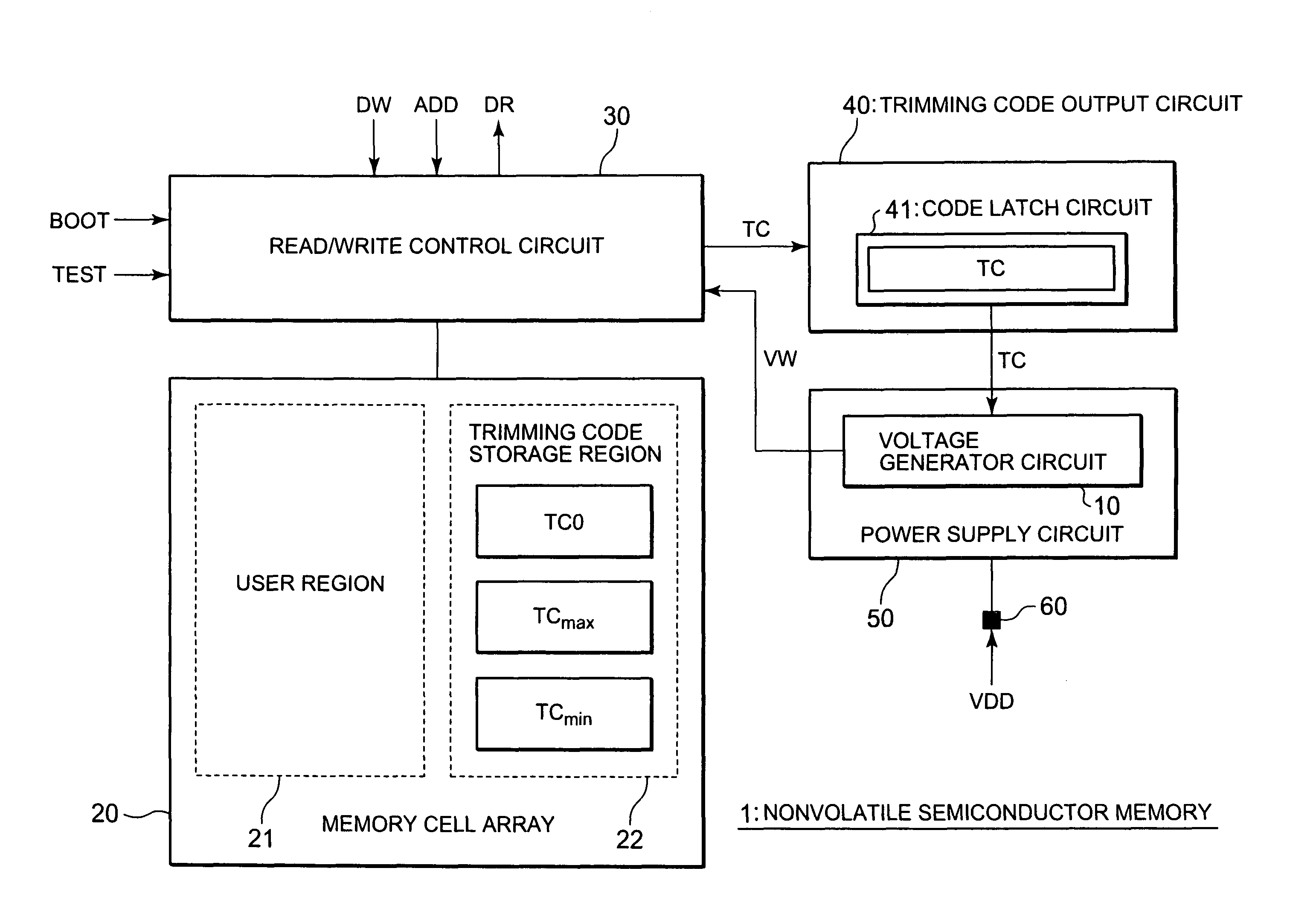
[0028]A nonvolatile semiconductor memory according to the first exemplary embodiment is formed of a flash memory, an EEPROM, and so on, and internally generates a drive voltage for data read and write. To achieve this, the nonvolatile semiconductor memory according to the first exemplary embodiment is equipped with “a voltage generator circuit” for generating the drive voltage. The voltage generator circuit generally employs a charge pump or a voltage regulator.

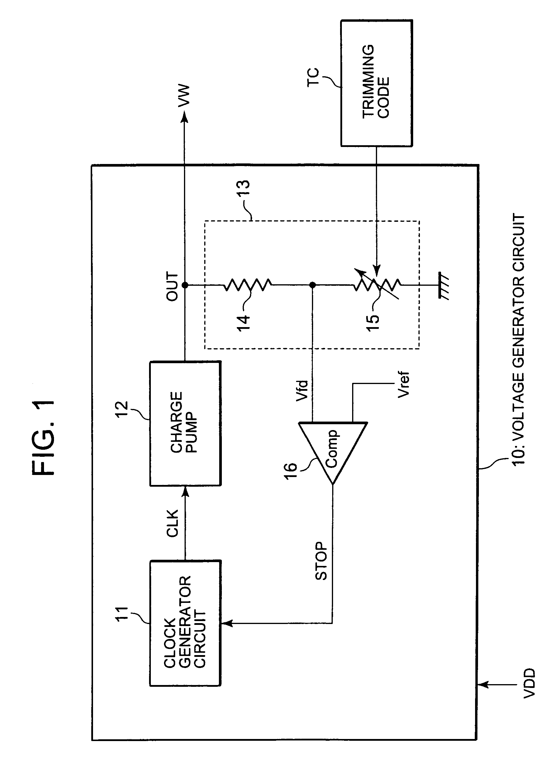
[0029]FIG. 1 is a block diagram illustrating an example of a voltage generator circuit 10 according to the first exemplary embodiment of the present invention. The voltage generator circuit 10 shown in FIG. 1 is a typical circuit using a charge pump. In more detail, the voltage...

second exemplary embodiment

[0085]FIG. 8 shows a nonvolatile semiconductor memory 1 according to a second exemplary embodiment. In the second exemplary embodiment, only the appropriate trimming code TCO is stored in the trimming code storage region 22 of the memory cell array 20. On the other hand, a bit operational circuit 70 is added as compared with the configuration shown in FIG. 5. The bit operational circuit 70 converts the appropriate trimming code TCO into the test trimming code TCmax or TCmin through bit operation (code up / code down). The bit operational circuit 70 is realized by a shift register, for example.

[0086]In testing the nonvolatile semiconductor memory 1, the read / write control circuit 30 reads the appropriate trimming code TCO from the memory cell array 20 in response to the test control signal TEST. Then, the read / write control circuit 30 outputs the read appropriate trimming code TCO to the bit operational circuit 70. Also, the read / write control circuit 30 outputs an operation control si...


PUM


Abstract

A nonvolatile semiconductor memory includes a nonvolatile memory array, a voltage generator circuit that generates a drive voltage which changes depending on a supply voltage and a trimming code, a control circuit that applies the generated drive voltage to the nonvolatile memory array, and a trimming code output circuit that outputs any one of plural trimming codes to the voltage generator circuit. The plural trimming codes include a test trimming code in addition to an appropriate trimming code for generating a desired drive voltage. The test trimming code is different from the appropriate trimming code, and used only in the test state. In the test state, the trimming code output circuit outputs the test trimming code to the voltage generator circuit, and the voltage generator circuit generates the drive voltage according to the test trimming code. In states other than the test state, the trimming code output circuit outputs the appropriate trimming code to the voltage generator circuit, and the voltage generator circuit generates the drive voltage according to the appropriate trimming code.

Description

INCORPORATION BY REFERENCE[0001]This application is based upon and claims the benefit of priority from Japanese Patent Application No. 2008-311970 which was filed on Dec. 8, 2008, the disclosure of which is incorporated herein in its entirety by reference.BACKGROUND OF THE INVENTION[0002]1. Field of the Invention[0003]The present invention relates to a nonvolatile semiconductor memory and a method for testing the nonvolatile semiconductor memory. In particular, the present invention relates to a nonvolatile semiconductor memory that internally generates a drive voltage for data read and write, and a method for testing the nonvolatile semiconductor memory.[0004]2. Description of Related Art[0005]There have been known nonvolatile semiconductor memories such as a flash memory or an electrically erasable and programmable read only memory (EEPROM). A memory cell of the nonvolatile semiconductor memory of this type has a charge storage layer such as a floating gate. The data write and era...

Claims


Application Information

Patent Timeline
Patent Type & Authority Patents(United States)
IPC IPC(8): G11C7/00
CPCG11C5/145G11C29/02G11C29/021G11C29/028
Inventor OKU, SATORU
Owner RENESAS ELECTRONICS CORP
Features
  • R&D
  • Intellectual Property
  • Life Sciences
  • Materials
  • Tech Scout
  • Unparalleled Data Quality
  • Higher Quality Content
  • 60% Fewer Hallucinations
Learn More