

Display device and manufacturing method thereof for minimizing inflow of oxygen and moisture from the outside
a technology of a display device and a manufacturing method, which is applied in the manufacture of electrode systems, electric discharge tubes/lamps, discharge tubes luminescent screens, etc., can solve the problems of deteriorating reducing the performance and the lifespan and affecting the efficiency of the organic emission layer. , to achieve the effect of reducing the inflow of oxygen
- Summary
- Abstract
- Description
- Claims
- Application Information
AI Technical Summary
Benefits of technology
Problems solved by technology
Method used
Image

Examples
first embodiment
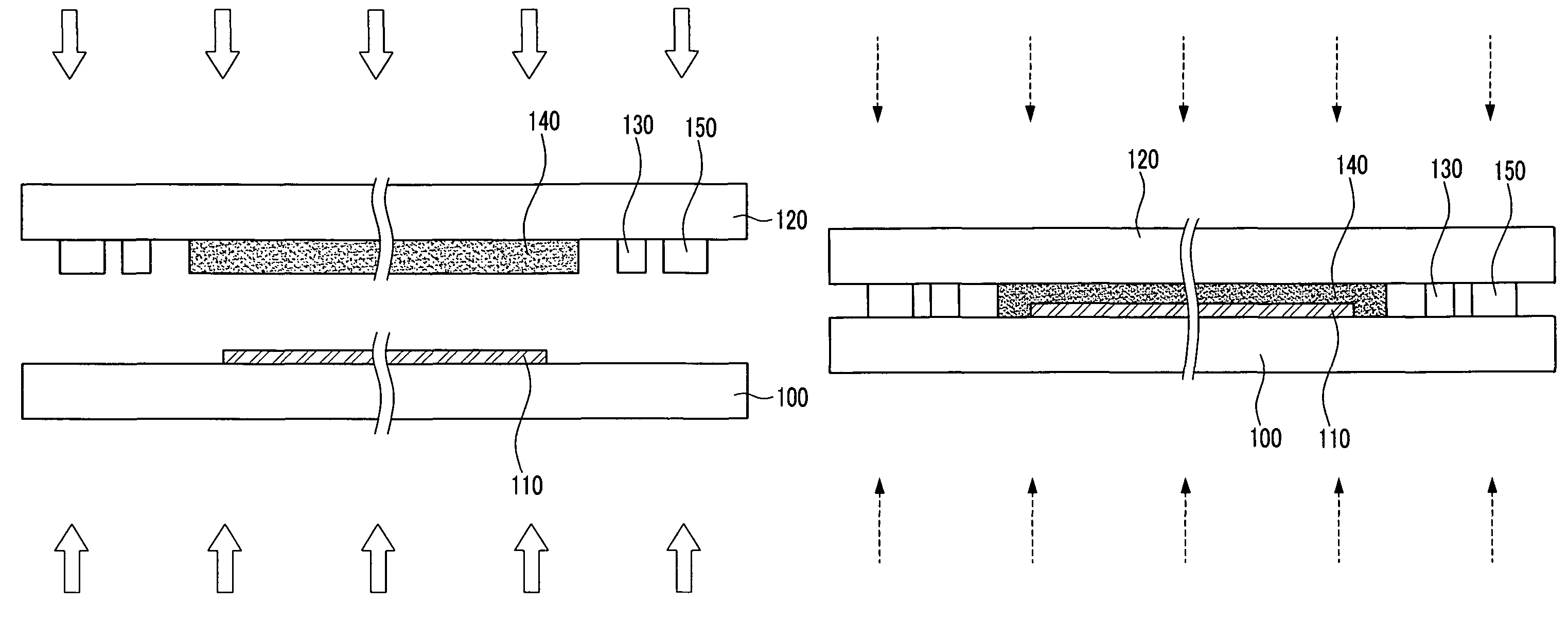
[0031]Referring to FIGS. 1 and 2, the present invention will be explained.
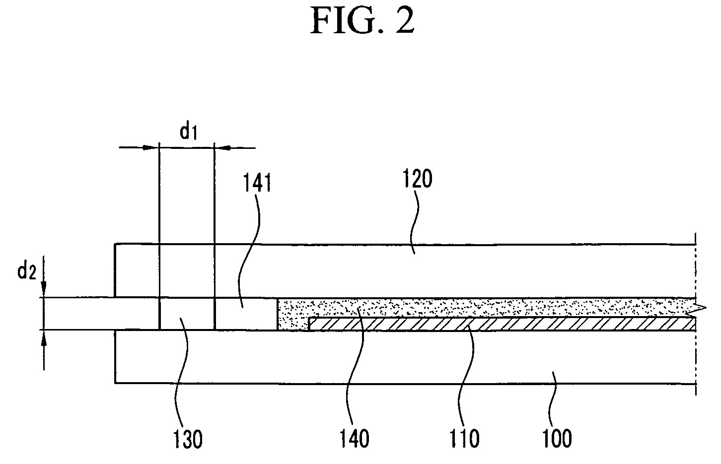
[0032]FIG. 1 illustrates a structure of a display device according to the first embodiment of the present invention and FIG. 2 illustrates a cross-section II-II of FIG. 1.
[0033]An OLED 1 includes an insulating substrate 100 and a cover plate 120 which are encapsulated by a sealant 130. An array of display elements 110 is disposed on the insulating substrate 100 and is covered by a protection film 140 on the cover substrate 120.
[0034]The insulating substrate 100 is transparent, and may be made of glass or plastic material. Further, a barrier layer (not shown) may be formed on the insulating substrate 100, i.e., between an array of display elements 110 and the insulating substrate 100. The barrier layer prevents oxygen or moisture from being introduced into the array of display elements 110 through the insulating substrate 100, and may include SiON, SiO2, SiNx, Al2O3, etc. The barrier layer can be formed by a sp...
second embodiment
[0059]Referring to FIGS. 4a and 4b, the present invention will be explained. A distinctive feature of this embodiment is an auxiliary sealant 150 outside the sealant 130.
[0060]After forming the sealant 130 and the protection film 140 on the cover substrate 120 as explained with FIG. 3b, the auxiliary sealant 150 made of epoxy resin et al. is formed on the cover substrate 120.
[0061]Next, as shown in FIG. 4a, the substrates 100 and 120 are joined together in a vacuum state. In this embodiment of the invention the vacuum is around 300 torr.
[0062]The auxiliary sealant 150 is cured by UV radiation. The pressure is then adjusted to atmospheric pressure to press the substrates 100 and 120 together creating a tight bond. After that, the sealant 130 is heated by laser radiation to seal the two substrates 100 and 120.
[0063]Next, as shown in FIG. 4b, the sealed substrates 100 and 120 are heated at a temperature of 150° C., and the protection film 140 becomes more transparent and thinner. There...
third embodiment
[0065]Referring FIGS. 5a and b, the present invention will be explained. Distinctive features of this embodiment are a desiccant 160 inside the sealant 130.
[0066]In addition to the sealant 130, the desiccant 160 can protect the display elements 110 from the inflow of oxygen and moisture.
[0067]The desiccant 160 may include Barium (Ba) or Calcium (Ca).
[0068]After forming the sealant 130, the protection film 140 and the auxiliary sealant 150 on the cover substrate 120 as explained with respect to FIG. 4b, the desiccant 160 is formed on the cover substrate 120 using a dispensing method or screen printing method.
[0069]Next, as shown in FIG. 5a, the substrates 100 and 120 are joined together in a vacuum. In one embodiment of the invention the vacuum is around 300 torr. The auxiliary sealant 150 is cured by UV radiation. The pressure is then adjusted to atmospheric pressure to press the substrates 100 and 120 together creating a tight bond. After that, the sealant 130 is heated by laser ra...
PUM
 Abstract
Description
Claims
Application Information