

LED chip package structure using a substrate as a lampshade and method for making the same
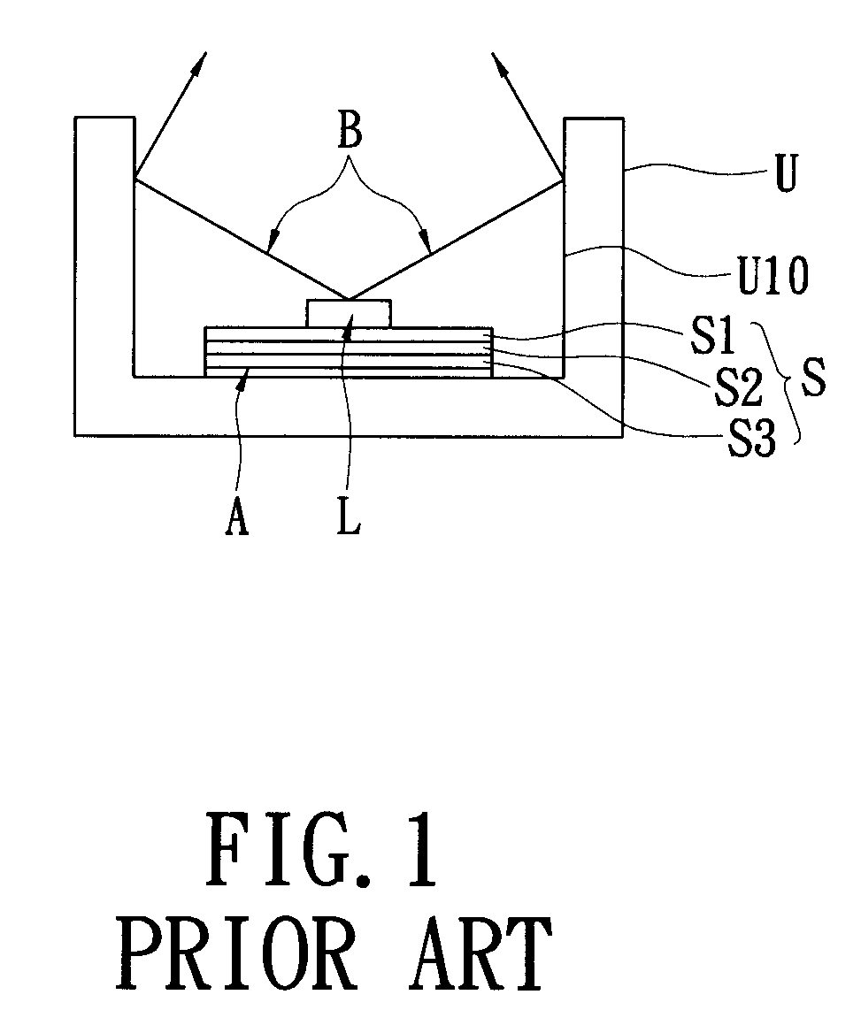
a technology of led chips and lampshade, which is applied in the direction of semiconductor devices for light sources, lighting and heating devices, lighting support devices, etc., can solve the problems of complex process for disposing led package structures inside lampshade u, and achieve the effect of increasing heat dissipation effect and high heat-transmitting efficiency
- Summary
- Abstract
- Description
- Claims
- Application Information
AI Technical Summary
Benefits of technology
Problems solved by technology
Method used
Image

Examples
first embodiment
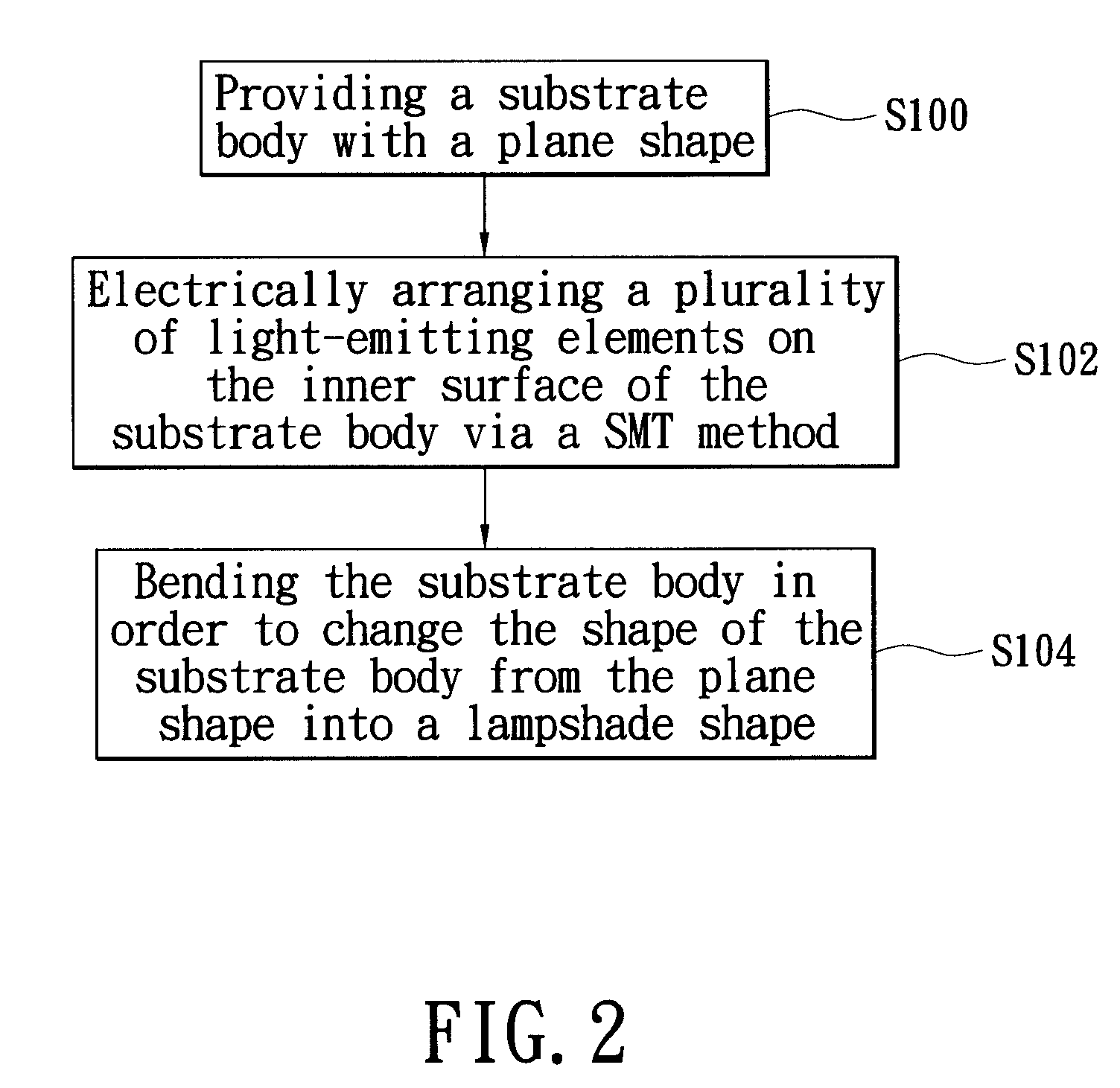
[0023]Referring to FIGS. 2 and 2A to 2C2, the present invention provides a method for making an LED chip package structure using a substrate as a lampshade.
[0024]The method of the present invention includes: referring to FIGS. 2 and 2A, providing a substrate body 1a with a plane shape (S100). The substrate body 1a has a positive trace 10a and a negative trace 11a respectively formed on the inner surface 100a of the substrate body 1a. The substrate body 1a has a metal layer 12a and a Bakelite layer 13a formed on the metal layer 12a. Both the positive trace 10a and the negative trace 11a can be aluminum circuits or silver circuits. In addition, the substrate body 1a can be a PCB (Printed Circuit Board), a flexible substrate, an aluminum substrate, a ceramic substrate, or a copper substrate.
[0025]Referring to FIGS. 2 and 2B, the method further includes: electrically arranging a plurality of light-emitting elements 2a on the inner surface 100a of the substrate body 1a via a SMT (Surface...
second embodiment
[0027]Referring to FIGS. 3 and 3A to 3C2, the present invention provides a method for making an LED chip package structure using a substrate as a lampshade.
[0028]The method of the present invention includes: referring to FIGS. 3 and 3A, providing a substrate body 1b with a plane shape (S200). The substrate body 1b has a positive trace 10b and a negative trace 11b respectively formed on the inner surface 100b of the substrate body 1b. The substrate body 1b has a metal layer 12b and a Bakelite layer 13b formed on the metal layer 12b. Both the positive trace 10b and the negative trace 11b can be aluminum circuits or silver circuits. In addition, the substrate body 1b can be a PCB (Printed Circuit Board), a flexible substrate, an aluminum substrate, a ceramic substrate, or a copper substrate.
[0029]Referring to FIGS. 3 and 3B, the method further includes: bending the substrate body 1b in order to change the shape of the substrate body 1b from the plane shape into a lampshade shape (S202)...
third embodiment
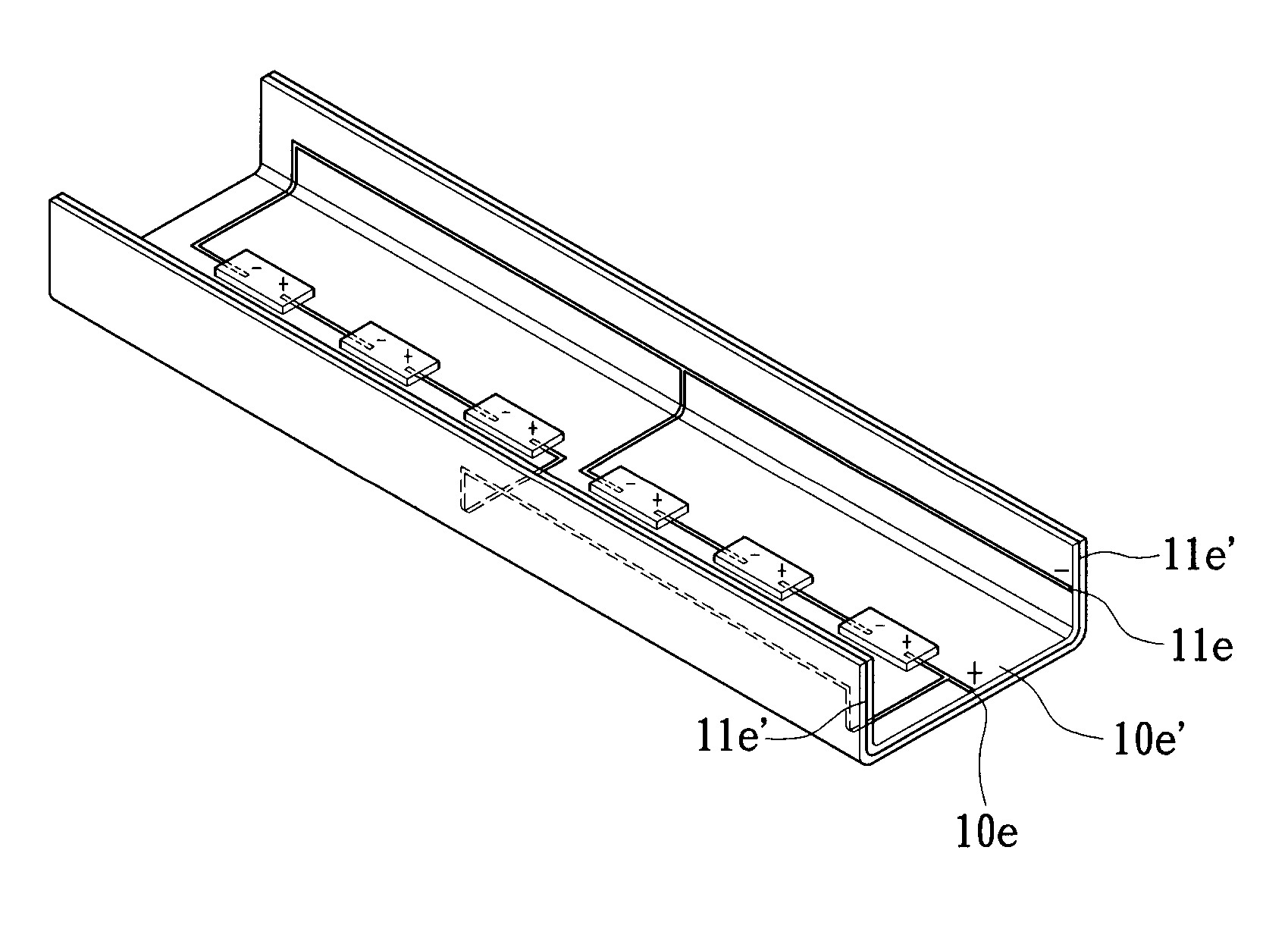
[0033]Referring to FIGS. 4 and 4A to 4C2, the present invention provides a method for making an LED chip package structure using a substrate as a lampshade.
[0034]The method of the present invention includes: referring to FIGS. 4 and 4A, providing a substrate body 1c with a plane shape, and the substrate body 1c having two concave portions 14c (S300). The substrate body 1c has a positive trace 10c and a negative trace 11c respectively formed on the inner surface 100c of the substrate body 1c. The substrate body 1c has a metal layer 12c and a Bakelite layer 13c formed on the metal layer 12c. In addition, each concave portion 14c is a continuous concave groove.
[0035]Referring to FIGS. 4 and 4B, the method further includes: bending the substrate body 1c along the two concave portions 14c in order to change the shape of the substrate body 1c from the plane shape into a lampshade shape (S302). In other words, the substrate body 1c is bent into a substrate body 1c′ with lampshade shape, an...
PUM
 Abstract
Description
Claims
Application Information