Inductor device, and method of manufacturing the same

a technology of inductor and inductor body, which is applied in the direction of magnets, inductances, magnetic bodies, etc., can solve the problems of increased production costs, increased production costs, and additional costs for designing dedicated components, etc., and achieves high reliability and easy formation

Active Publication Date: 2011-08-23
SHINKO ELECTRIC IND CO LTD
View PDF15 Cites 2 Cited by
  • Summary
  • Abstract
  • Description
  • Claims
  • Application Information

AI Technical Summary

Benefits of technology

[0013]It is an object of the present invention to provide an inductor device that can be formed to make the inductor element with high reliability build in, and a method of manufacturing the same.
[0015]In the inductor device of the present invention, the first and second magnetic body pattern layers (such as the Ni Co layer, or the like) are arranged to the upper and lower side of the planar coil layer, and the first and second magnetic body pattern layers are made to patterns by providing slits. Accordingly, in the case that this inductor device is applied to the printed-wiring board, or the like, the EMI noise is reduced and high reliability can be assured, and also an inductance can be increased. Also, since the first and second magnetic body pattern layers are arranged to intersect orthogonally with the planar coil layer, generation of the eddy current can be suppressed in contrast to the case where the pattern layers do not intersect orthogonally with the planar coil layer.
[0017]Also, even when the inductor device is applied to the high-frequency circuit, there is no necessity that the inductor component which is designed particularly for high-frequency purpose should be employed. Therefore, a manufacturing cost can be reduced.
[0019]By employing the above approach, the magnetic body pattern layer which is patterned and has arbitrary film thickness can be formed easily on the catalyst metal-containing resin pattern layer by the electroless plating, without etching the magnetic body layer having film property that is hard to etch.
[0020]As explained above, the inductor device of the present invention can be formed to make the inductor element with high reliability built in.

Problems solved by technology

Also, a cost of such inductor component is relatively high, and thus it is possible that an increase in production cost is caused.
Hence, an additional cost is required to design the dedicated component.
However, according to this method, such problems existed that the EMI (undesirable radiation) noise is emitted from the inductor element or the sufficient characteristics of the inductor element cannot be obtained, so that the reliability of the inductor element is not always satisfactory.

Method used


Image

  • Inductor device, and method of manufacturing the same
  • Inductor device, and method of manufacturing the same
  • Inductor device, and method of manufacturing the same

Examples


first embodiment

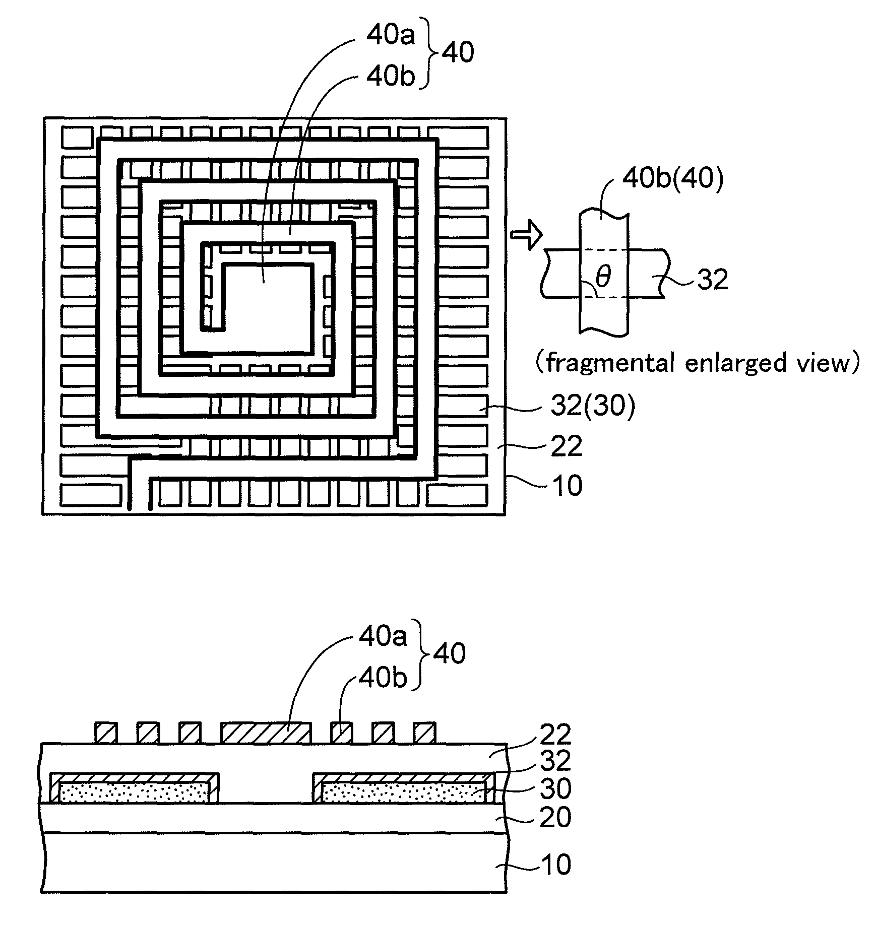
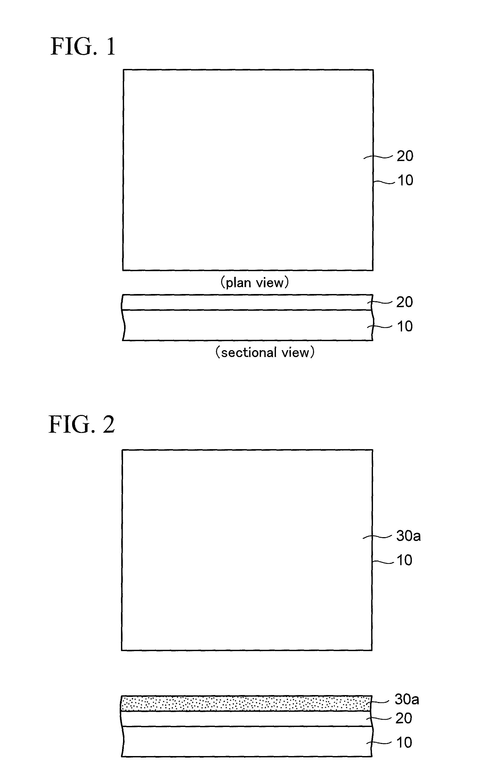
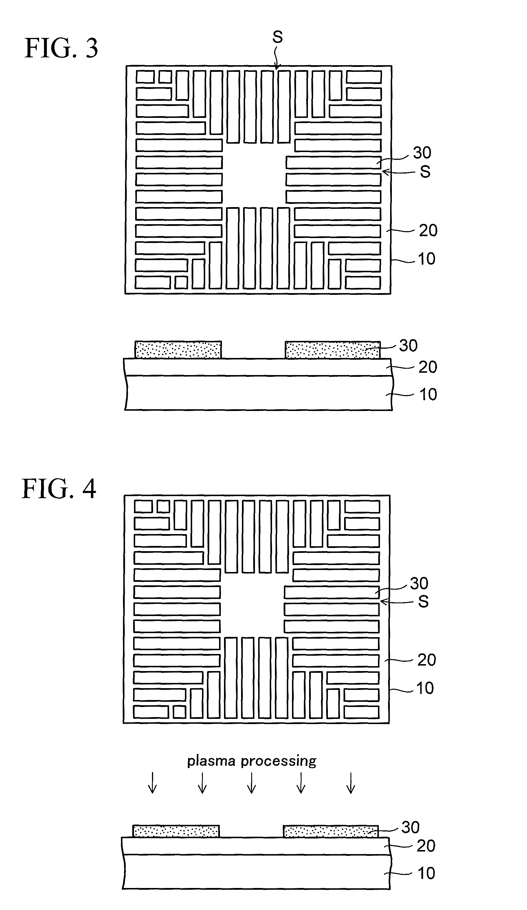
[0038]FIG. 1 to FIG. 12 are plan views and sectional views showing a method of manufacturing an inductor device according to a first embodiment of the present invention respectively. In FIG. 1 to FIG. 12, upper views are a plan view respectively, and lower views are a sectional view respectively.

[0039]In the method of manufacturing the inductor device in the first embodiment, as shown in FIG. 1, first, a first insulating layer 20 is formed on a substrate 10. The first insulating layer 20 is formed of an epoxy resin or a polyimide resin, and that thickness is set to 20 to 200 μm. The first insulating layer 20 is formed by either pasting a resin film on the substrate 10 or coating a liquid resin on the substrate 10.

[0040]Preferably the substrate 10 is the wiring substrate having the wiring layer. As described later, the inductor element connected to the wiring layer is built-in over the substrate 10.

[0041]Then, as shown in FIG. 2, a photosensitive catalyst metal-containing resin layer...

second embodiment

[0094]FIGS. 13A to 13D, FIGS. 14A and 14B, FIG. 15, and FIG. 16 are sectional views showing a method of manufacturing an inductor device according to a second embodiment of the present invention respectively. A feature of the second embodiment resides in that the first and second Ni Co pattern layers arranged to the upper and lower side are brought partially close to each other by providing the holes in the insulating layer, thereby a magnetic coupling is increased.

[0095]In the method of manufacturing the inductor device in the second embodiment, as shown in FIG. 13A, first, an insulating substrate 50 (intermediate insulating layer) whose thickness is 100 to 150 μm is prepared. Then, a through hole TH which penetrates to the thickness direction is formed in the insulating substrate 50 by the drilling, or the like.

[0096]Then, as shown in FIG. 13B, the first and second planar coil layers 40, 42 made of copper, or the like are formed on both surface sides of the insulating substrate 50...


PUM

PropertyMeasurementUnit
aspect ratioaaaaaaaaaa
thicknessaaaaaaaaaa
thicknessaaaaaaaaaa

Abstract

An inductor device includes a first magnetic body pattern layer in which slits are provided and which is made to a pattern, a lower insulating layer formed on the first magnetic body pattern layer, a planar coil layer formed on the lower insulating layer, an upper insulating layer formed on the planar coil layer, and a second magnetic body pattern layer formed on the upper insulating layer and in which slits are provided and which is made to a pattern, wherein the first magnetic body pattern layer and the second magnetic body pattern layer are arranged to intersect orthogonally with the planar coil layer.

Description

CROSS-REFERENCE TO RELATED APPLICATIONS[0001]This application is based on and claims priority of Japanese Patent Application No. 2009-057414 filed on Mar. 11, 2009, the entire contents of which are incorporated herein by reference.BACKGROUND OF THE INVENTION[0002]1. Field of the Invention[0003]The present invention relates to an inductor device and a method of manufacturing the same and, more particularly, an inductor device including such a structure that a planar type inductor is formed on a wiring substrate, or the like and a method of manufacturing the same.[0004]2. Description of the Related Art[0005]In the prior art, there is the inductor device which is used in the high-frequency circuit, and the like in various electronic equipments. As the structure of the inductor, there is the winding wire type in which the electrical wire is wound, or the planar type in which the spiral coil conductor is formed on a plane, and the like.[0006]In Patent Literature 1 (Patent Application Pub...

Claims


Application Information

Patent Timeline
Patent Type & Authority Patents(United States)
IPC IPC(8): H01F5/00
CPCH01F17/0013H01F41/046Y10T29/49073Y10T29/4902H01F2017/008
Inventor MASHINO, NAOHIRO
Owner SHINKO ELECTRIC IND CO LTD
Why Eureka
Try Eureka