Photomask

a technology of photomasks and masks, applied in the field of photomasks, can solve problems such as affecting the formation of predetermined patterns in the fabrication of semiconductor devices, and achieve the effect of reducing the potential difference between patterns

Inactive Publication Date: 2011-08-30
SONY CORP
View PDF5 Cites 0 Cited by
  • Summary
  • Abstract
  • Description
  • Claims
  • Application Information

AI Technical Summary

Benefits of technology

[0014]It is therefore desirable to provide a photomask having an island-shaped independent light shielding pattern, in which the deformation of the pattern due to electrostatic damage can be prevented or reduced.
[0016]In a photomask according to an embodiment of the present invention, a slit which is a region with no metal pattern is defined around a chip pattern region. Thus, a plurality of chip pattern regions defined on a base are separated from one another by slits. Therefore, for example, even when an island-shaped isolated light shielding pattern is defined in a chip pattern region, the difference can be reduced between an area of the isolated light shielding pattern and an area of a light shielding pattern defined around the isolated light shielding pattern can be reduced.
[0017]The reduction in the difference between the isolated light shielding pattern and the pattern defined therearound can reduce the potential difference between the patterns even when the metal material of the light shielding pattern is charged due to static electricity or the like.
[0018]According to an embodiment of the present invention, therefore, a photomask in which even when an island-shaped isolated light shielding pattern is defined, the deformation of the pattern due to the electrostatic damage caused between the island-shaped isolated light shielding pattern and a light shielding pattern defined therearound can be prevented or reduced can be achieved.

Problems solved by technology

Exposure using a photomask in which electrostatic damage has occurred may impair the formation of a predetermined pattern in the fabrication of semiconductor devices or the like.

Method used


Image

  • Photomask
  • Photomask
  • Photomask

Examples


first embodiment

[0028]A photomask according to a first embodiment of the present invention will now be described.

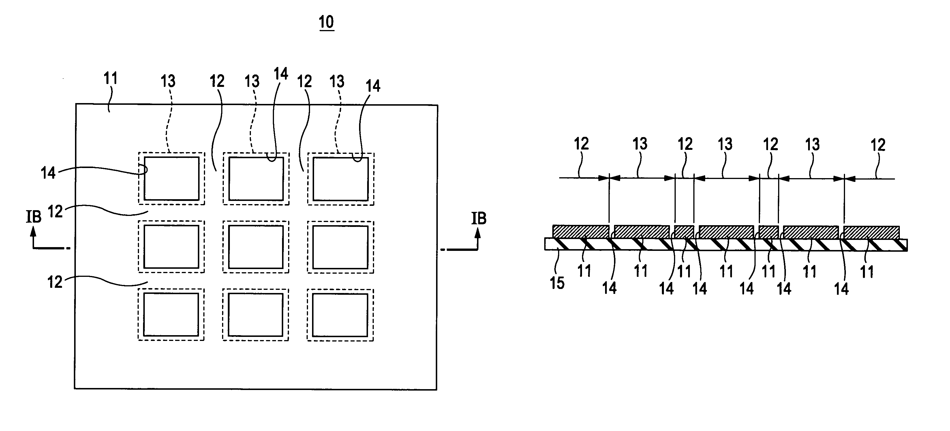
[0029]FIG. 1A is a schematic configuration diagram of a photomask 10 according to the first embodiment. FIG. 1B is a cross-sectional view taken along the line IB-IB of FIG. 1A.

[0030]The photomask 10 shown in FIG. 1A may be a multichip photomask (or multi-layer photomask or multi-product photomask) for fabricating semiconductor devices.

[0031]The photomask 10 has a light shielding pattern 11 defined on substantially an entire surface thereof. The light shielding pattern 11 may be composed of a metal material such as chromium, molybdenum, tungsten, aluminum, or nickel. The photomask 10 also includes a plurality of chip pattern regions 13 in accordance with a layout of semiconductor devices on a base (transparent substrate) (hereinafter referred to simply as a “base”). In FIG. 1A, the chip pattern regions 13 are indicated by broken lines. The light shielding pattern 11 is defined over the ch...

second embodiment

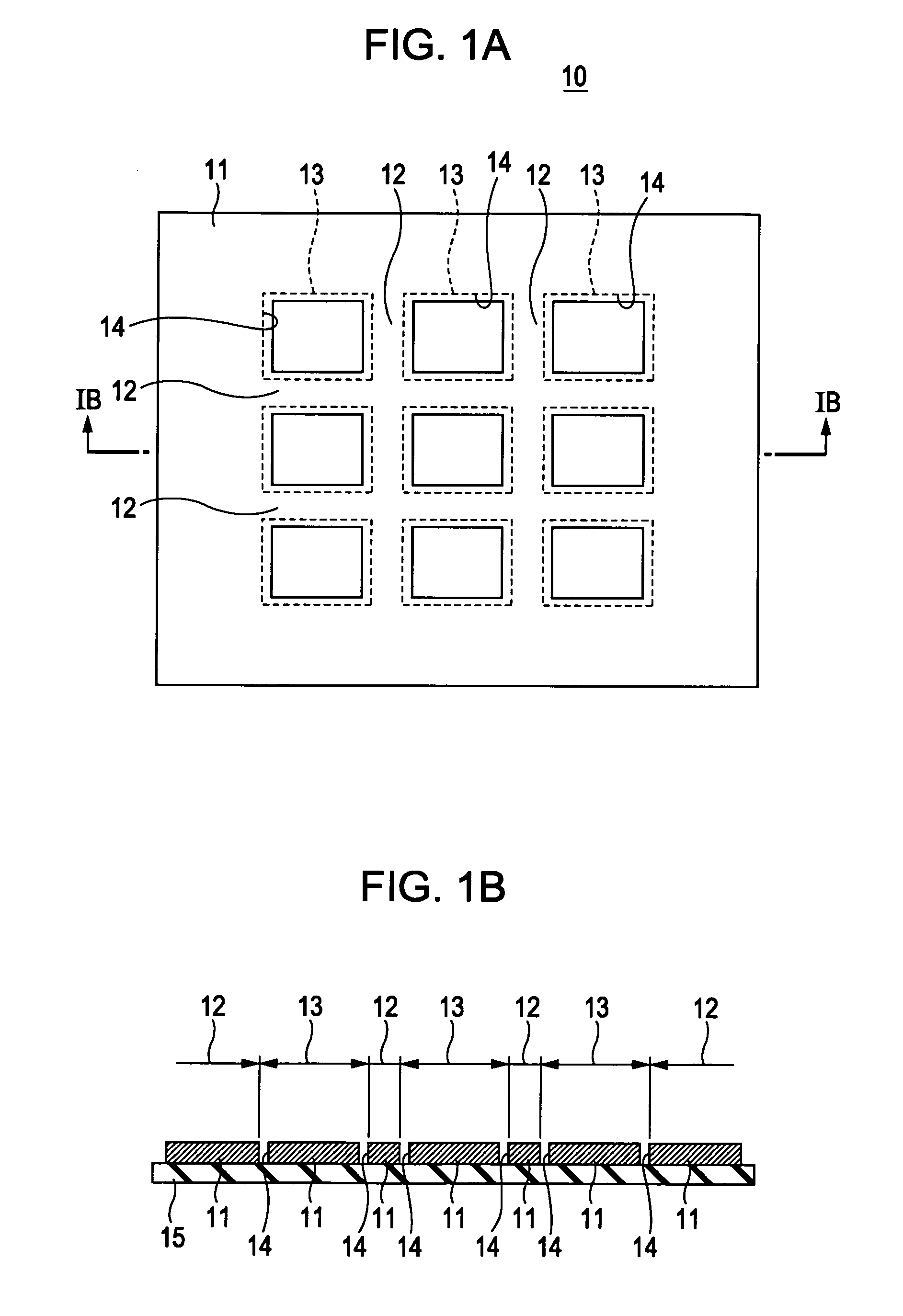
[0049]FIG. 2 is a schematic configuration diagram of a photomask 20 according to a second embodiment of the present invention. In FIG. 2, components similar to those of the photomask 10 shown in FIGS. 1A and 1B are assigned the same reference numerals, and detailed descriptions thereof are omitted.

[0050]Like the photomask 10 shown in FIG. 1A, the photomask 20 shown in FIG. 2 may be a multichip photomask (or multi-layer photomask or multi-product photomask) for fabricating semiconductor devices.

[0051]The photomask 20 has a light shielding pattern 11 of metal such as chromium defined on substantially an entire surface thereof. The photomask 20 also includes a plurality of chip pattern regions 13 in accordance with a layout of semiconductor devices on a base. In FIG. 2, the chip pattern regions 13 are indicated by broken lines. The light shielding pattern 11 is defined over the chip pattern regions 13 in accordance with a layout such as an arrangement of elements or a circuit pattern o...

third embodiment

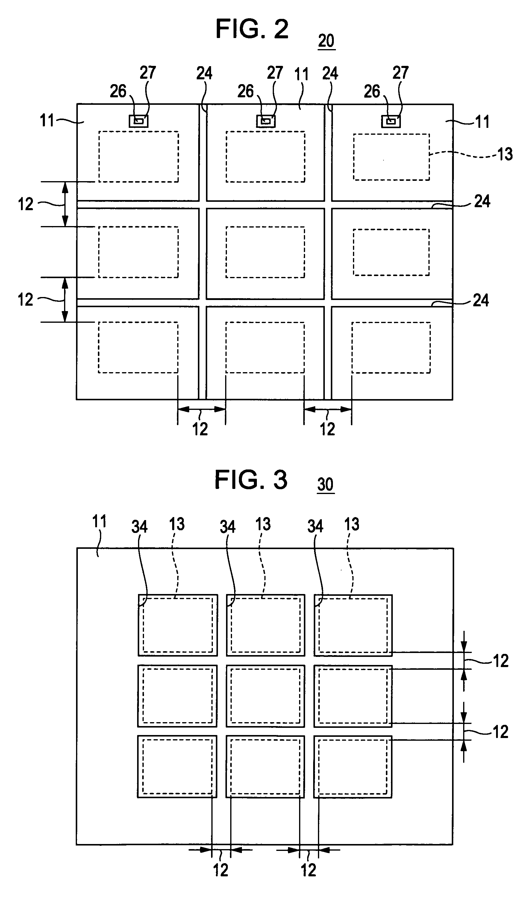
[0062]FIG. 3 is a schematic configuration diagram of a photomask 30 according to a third embodiment of the present invention. In FIG. 3, components similar to those of the photomask 10 shown in FIGS. 1A and 1B are assigned the same reference numerals, and detailed descriptions thereof are omitted.

[0063]Like the photomask 10 shown in FIG. 1A, the photomask 30 shown in FIG. 3 may be a multichip photomask (or multi-layer photomask or multi-product photomask) for fabricating semiconductor devices.

[0064]The photomask 30 has a light shielding pattern 11 of metal such as chromium defined on substantially an entire surface thereof. The photomask 30 also includes a plurality of chip pattern regions 13 in accordance with a layout of semiconductor devices on a base. In FIG. 3, the chip pattern regions 13 are indicated by broken lines. The light shielding pattern 11 is defined over the chip pattern regions 13 in accordance with a layout such as an arrangement of elements or a circuit pattern of...


PUM

PropertyMeasurementUnit
widthaaaaaaaaaa
electrically non-conductiveaaaaaaaaaa
light shieldingaaaaaaaaaa

Abstract

A photomask includes a base, a plurality of chip pattern regions over which a light shielding pattern of a metal material is defined, the plurality of chip pattern regions being defined on the base, scribe regions defined between the chip pattern regions, the scribe regions being defined by using the light shielding pattern, and slits in which the light shielding pattern is not defined, the slits being defined so as to surround the chip pattern regions.

Description

BACKGROUND OF THE INVENTION[0001]1. Field of the Invention[0002]The present invention relates to a photomask of an exposure device, having a light shielding pattern, which is used in a photolithographic process for use in the fabrication of semiconductor devices.[0003]2. Description of the Related Art[0004]In a photolithographic process for fabricating semiconductor devices or the like, multichip photomasks are used. In a photomask, a layout such as an arrangement of elements or a circuit pattern of semiconductor devices is defined by using a light shielding pattern of metal or the like (see, for example, Japanese Unexamined Patent Application Publication Nos. 3-121456 and 5-19448).[0005]FIG. 5 shows a schematic configuration of a multichip photomask 50 for fabricating semiconductor devices.[0006]The photomask 50 shown in FIG. 5 has a light shielding pattern 51 of metal such as chromium (Cr) in accordance with a layout of semiconductor devices to be formed. The light shielding patte...

Claims


Application Information

Patent Timeline
Patent Type & Authority Patents(United States)
IPC IPC(8): G03F1/00G03F1/08G03F1/40G03F1/68
CPCG03F1/14G03F1/40G03F1/50
Inventor HATANO, KEISUKEMATSUNUMA, TAKESHIMIYAZAWA, SHINJI
Owner SONY CORP
Why Eureka
Try Eureka