
Laser process for side plating of terminals

a terminal and side plating technology, applied in the field of integrated circuit (ic) packages, can solve the problems of inability to visually inspect the solder joint between the terminal and the contact pad of the pcb, small silicon chips on which the integrated circuit is formed, and difficult handling, etc., to achieve the effect of saving the manufacturing process in general

Active Publication Date: 2011-09-13
ANALOG DEVICES INT UNLTD
View PDF11 Cites 28 Cited by
  • Summary
  • Abstract
  • Description
  • Claims
  • Application Information

AI Technical Summary

Benefits of technology

[0007]There is a need for a lower-cost method of creating a notch in the connecting bars of a leadframe during the IC package manufacturing process. Use of a laser to remove mold compound from an etched groove eliminates the need for a half-depth saw cut after the IC packages have been overmolded and may produce a overall saving in the manufacturing process.

Problems solved by technology

The silicon chips on which integrated circuits are formed are so small that they are sensitive to damage and hard to handle, and many IC chips are packaged in enclosures that protect the chips and provide larger contact leads that can be attached to circuitry on substrates such as printed circuit boards (PCBs).
One difficulty with this type of package is that it is not possible to visually inspect the solder joint between the terminals and the contact pads of the PCB.
Saw blades are a significant expense in the manufacturing of IC packages and the need to perform the half-thickness saw cut prior to singulation adds cost to the manufacturing process.

Method used


Image

  • Laser process for side plating of terminals
  • Laser process for side plating of terminals
  • Laser process for side plating of terminals

Examples


Embodiment Construction

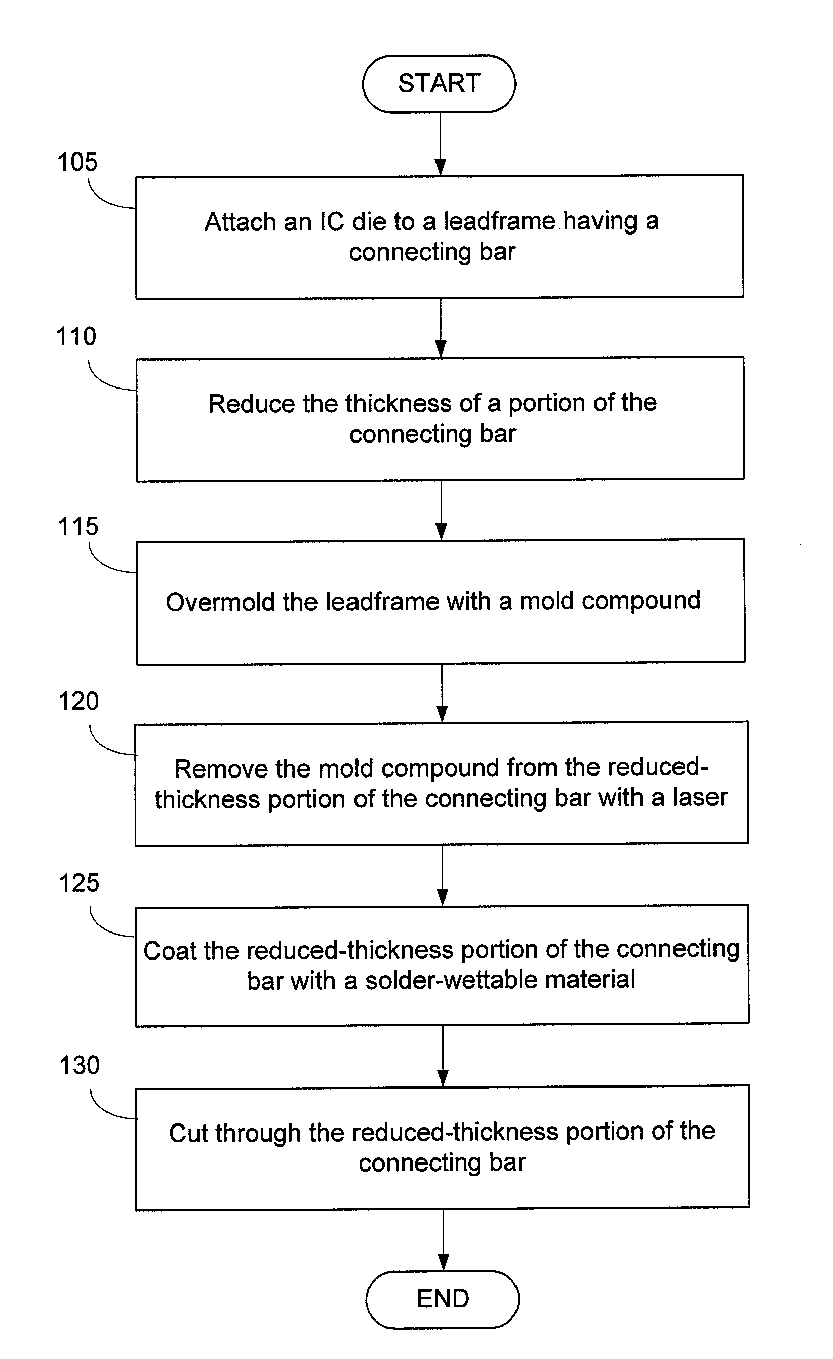
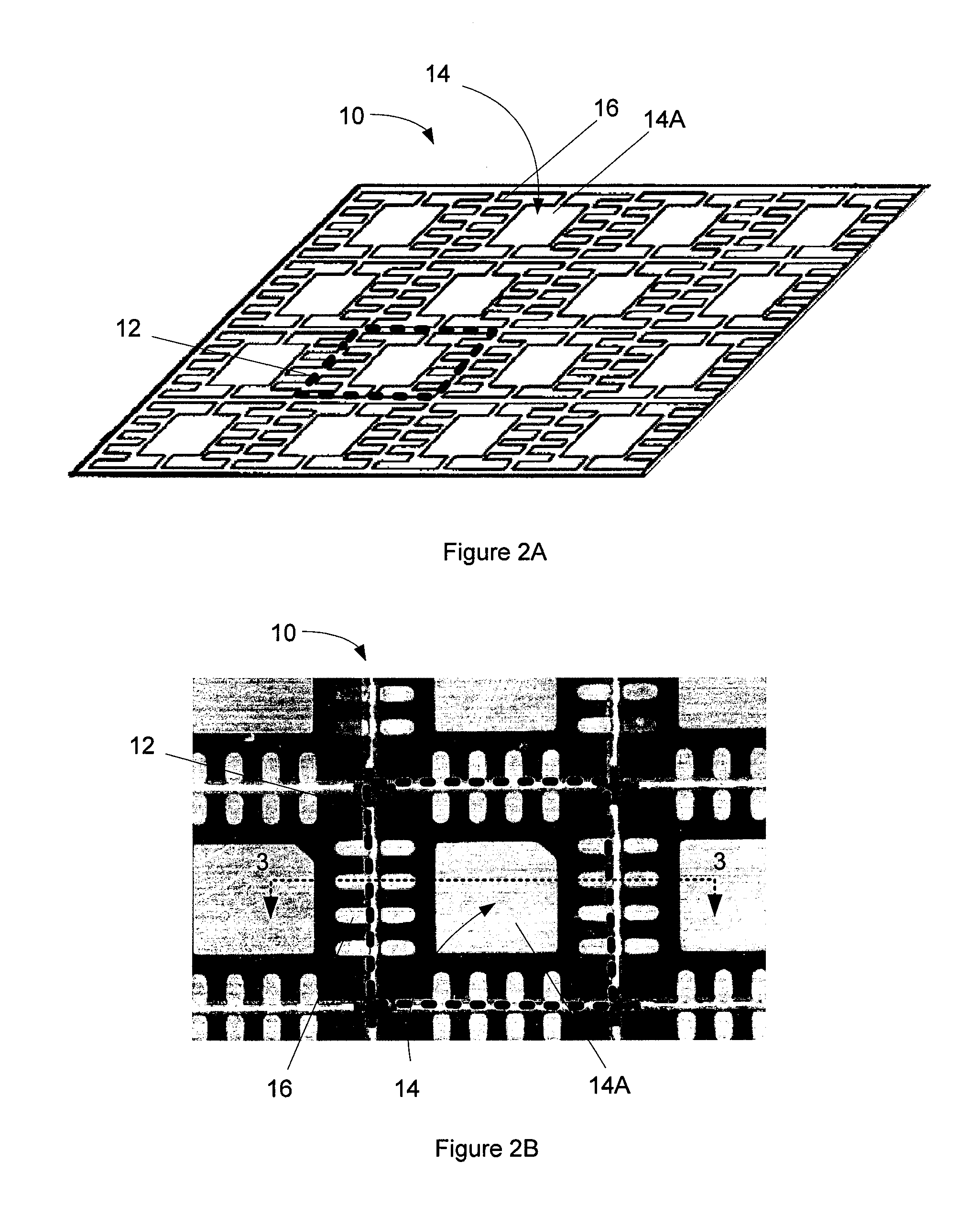
[0019]The methods disclosed herein describe how an IC package terminal may be beveled to create a visually inspectable solder joint when the IC package is soldered to a PCB. The process etches the connection bars in a frame in the areas where the individual IC packages will be singulated from the frame and utilizes a laser to clean the etched areas and remove any mold compound or other contaminant from the surface of the etched areas. Etching is frequently done to reduce the amount of metal to be cut in a later sawing process, extending the life of the saw and thereby reducing manufacturing cost. The cleaned etched areas are plated at the same time that the underside of the connection bars are plated with a solder-wettable metal. The IC packages are then singulated by cutting along the center of the etched areas with a narrow saw that leaves a portion of the etched area as a bevel at the lower outside corner of the terminals that are formed from the cut connection bars.

[0020]In the ...


PUM


Abstract

A method of preparing a portion of the side of a terminal of an Integrated Circuit (IC) package for solder is disclosed. The method comprises the steps of attaching an IC die to a leadframe comprising a connecting bar, reducing the thickness of a portion of the connecting bar, overmolding the leadframe with a mold compound, removing the mold compound from the reduced-thickness portion of the connecting bar using a laser, coating the reduced-thickness portion of the connecting bar with a solder-wettable material, and cutting through the thickness of the connecting bar within the reduced thickness portion of the connecting bar, wherein the cut has a width that is less than the width of the reduced thickness portion of the connecting bar.

Description

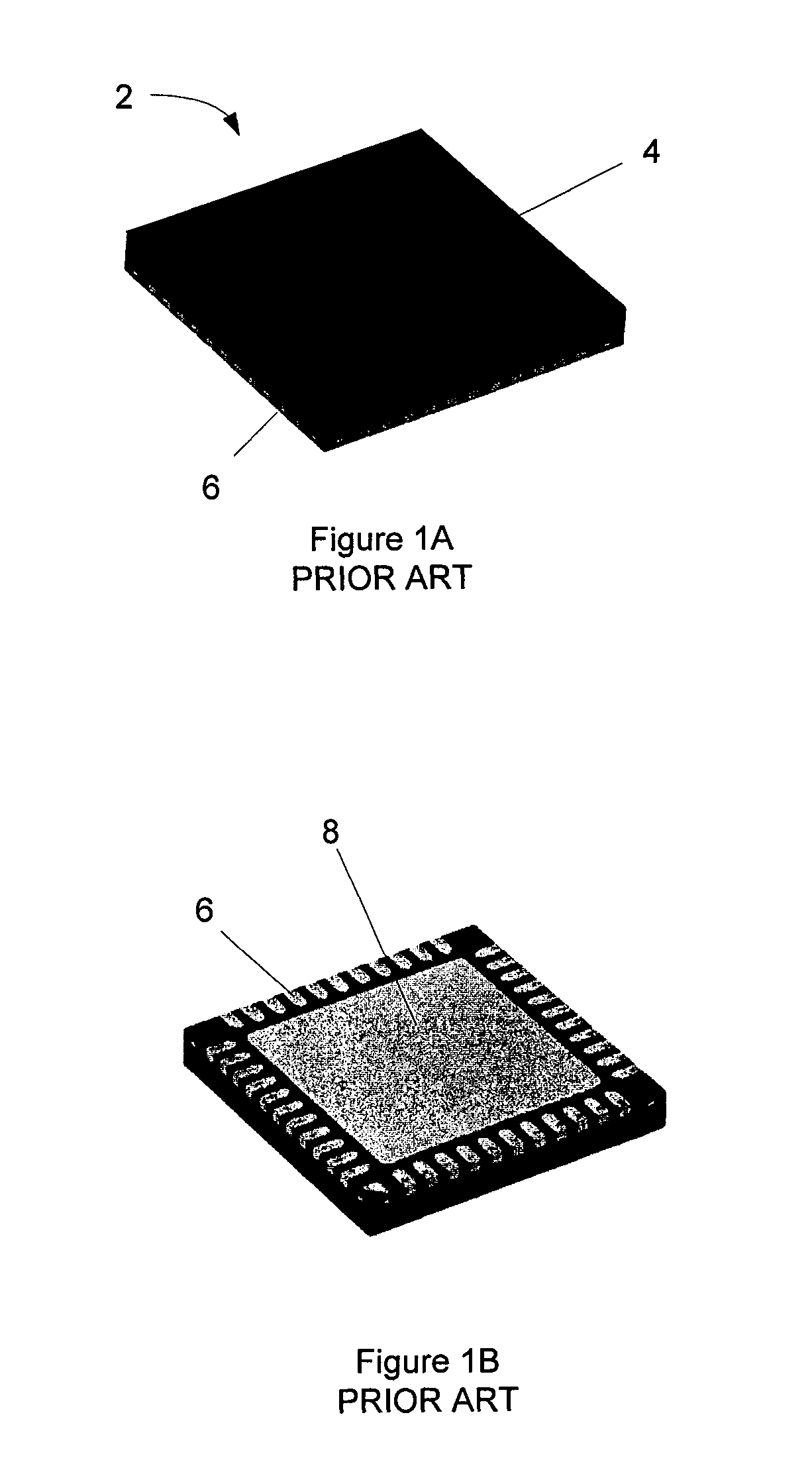
BACKGROUND[0001]1. Field[0002]The present disclosure generally relates to integrated circuit (IC) packages and, more particularly, to methods of plating and singulating IC packages.[0003]2. Description of the Related Art[0004]The silicon chips on which integrated circuits are formed are so small that they are sensitive to damage and hard to handle, and many IC chips are packaged in enclosures that protect the chips and provide larger contact leads that can be attached to circuitry on substrates such as printed circuit boards (PCBs). One common method of assembling an IC package of this type is to attach a “leadframe” as a mechanical support to the die during its assembly. A portion of the leadframe is trimmed off, leaving only the leads that provide the external connections for the finished product. A leadframe comprises a “die attach pad”, to which the die is attached, and “leads”, which provide external electrical connections. The die, adhesive, wires and leadframe are encased in ...

Claims


Application Information

Patent Timeline
Patent Type & Authority Patents(United States)
IPC IPC(8): H01L21/44
CPCH01L21/4821H01L21/561H01L23/49548H01L23/49582H01L24/97H01L23/3107H01L2924/00014H01L2924/10253H01L2224/45099H01L2924/00H01L2924/181H01L2924/14H01L23/48
Inventor OLSEN, EDWARD WILLIAM
Owner ANALOG DEVICES INT UNLTD
Learn More