Surface defect inspecting apparatus with defect detection optical system and defect-detected image processing

a defect detection and defect technology, applied in the direction of optically investigating flaws/contamination, measurement devices, instruments, etc., can solve the problems of disadvantageous requirements for circuits receiving signals from adjacent elements in the width direction of adjacent elements, and poor accuracy in terms of exact size and height of defects, etc., to achieve high accuracy

Inactive Publication Date: 2011-09-13
HITACHI HIGH-TECH CORP
View PDF7 Cites 19 Cited by
  • Summary
  • Abstract
  • Description
  • Claims
  • Application Information

AI Technical Summary

Benefits of technology

[0006]The present invention is directed to a surface defect inspecting apparatus, which can employ a small number of detectors and circuits to detect with high accuracy the size and the height of a concave defect or a convex defect on the surface of a face plate.
[0007]One aspect of the present invention is to provide a surface defect inspecting apparatus with a defect detection optical system and defect-detected image processing, including: an irradiating optical system of irradiating a light beam on a surface of a face plate of a disk mounted on a stage to scan the surface of the face plate; a light-receiving optical system including a shading filter having a shading difference causing an amount of specular reflection light from the face plate resulting from the light beam irradiated on the disk to be changed and receiving the specular reflection light that has transmitted the shading filter; and processing means for identifying a defect on the surface of the face plate from the change in amount of the specular reflection light that has transmitted the shading filter. Another aspect of the present invention is to provide a surface defect inspecting apparatus, which carries out a processing method according to kinds of defect from defect data obtained from the inspected surface of the face plate, so that defects having features on the surface of the face plate, e.g., stripe defects or circular arc defects can be detected and sizes or heights thereof can be measured with high accuracy.
[0009]When the irregular defects on the surface of the face plate are read out from the change in amount of light received by the light receiver through the filter having the shading difference, portions (spots and so forth) having different reflectance on the surface of the face plate may be detected as irregular defects. To deal with this possible problem, the change in reflectance on the surface is measured by separately arranging a light-receiving system using direct light-receiving elements apart from the light-receiving elements described above without having the specular reflection light from the surface of the face plate transmit the shading filter. By subtracting the amount of light used for measuring the change in specular reflectance from the amount of light received by the light-receiving elements through the shading filter having the shading difference, it is possible to accurately detect the irregular defects without being affected by the change in reflectance on the surface of the face plate.
[0010]In this case, the generated defect detection signal deviated from the position having the transmittance of 50% of the shading filter due to the inclination of the irregular defect on the surface typically causes two peaks such as positive and negative peaks to be generated on each of the recess and convex defects. With this arrangement, the size of the defect can be detected by the distance between these peaks. In addition, the reason why the concave defect or the convex defect causes two peaks to be generated lies in that any of both defects typically has a pair of lateral inclined portions in the scanning direction of R and θ. When the irradiation position (i.e., the coordinate position) where the positive and negative peaks of the defect detection signal are generated is detected, the distance between the peaks can be obtained, and the width or the area depending on the size of the defect can be easily calculated from the relationship between the distance and the irradiation position. The present invention can easily determine the continuity of the detected defects from the relationship between the coordinate position of the detected defects and the distance between the peaks with respect to the detected defects. With this determination, the width or the area can be easily calculated even with respect to some deformed defects of the concave defect or the convex defect. The present invention can take an average of absolute values of both positive and negative peaks to detect with high accuracy the depth of the concave defect or the height of the convex defect. As a result, the present invention can detect with high accuracy the size of the irregular defect on the surface of the face plate to implement the surface defect inspecting apparatus facilitating defect classification.
[0017]According to the present invention, a surface defect inspecting apparatus is provided, which can use a small number of detectors and circuits to detect with high accuracy the size and the height of the concave defect or the convex defect on the surface of the face plate.

Problems solved by technology

This is why plural circuits receiving signals from adjacent elements in the width direction of the adjacent elements are disadvantageously required in the related art.
Further, according to the technique disclosed in JP-A-Hei15 (2003)-35678, irregular defects are determined by the lens effect, so that the accuracy is not good in terms of exact size and height of the defect.

Method used


Image

  • Surface defect inspecting apparatus with defect detection optical system and defect-detected image processing
  • Surface defect inspecting apparatus with defect detection optical system and defect-detected image processing
  • Surface defect inspecting apparatus with defect detection optical system and defect-detected image processing

Examples


Embodiment Construction

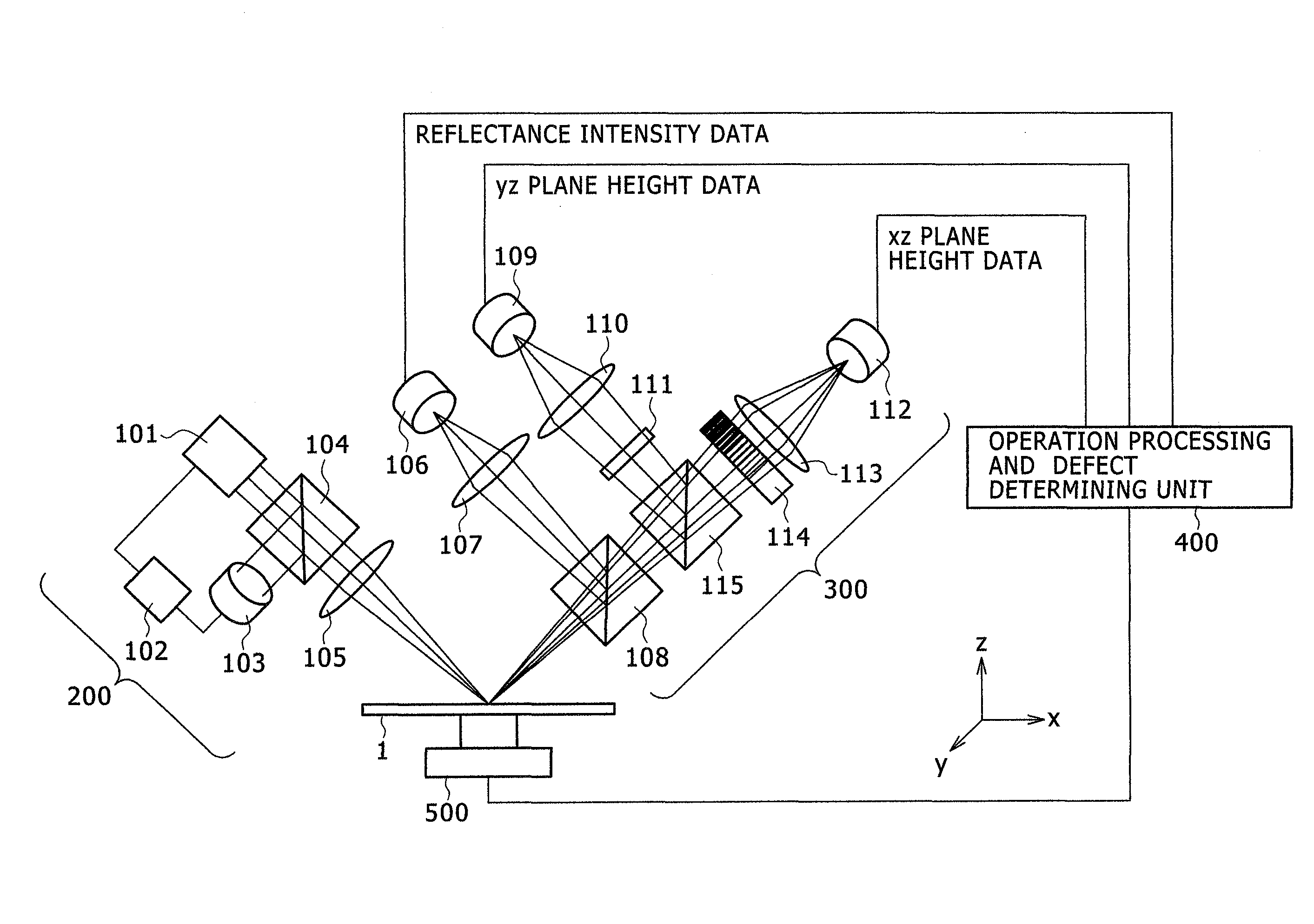
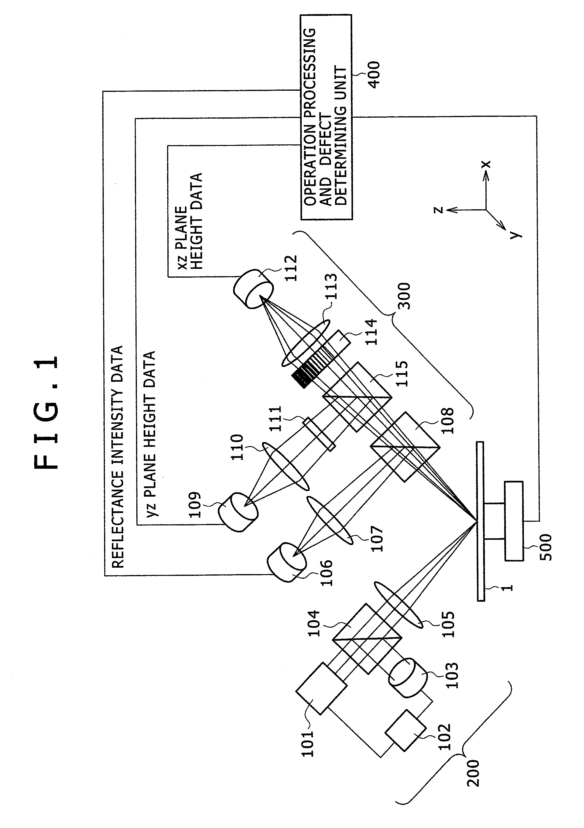
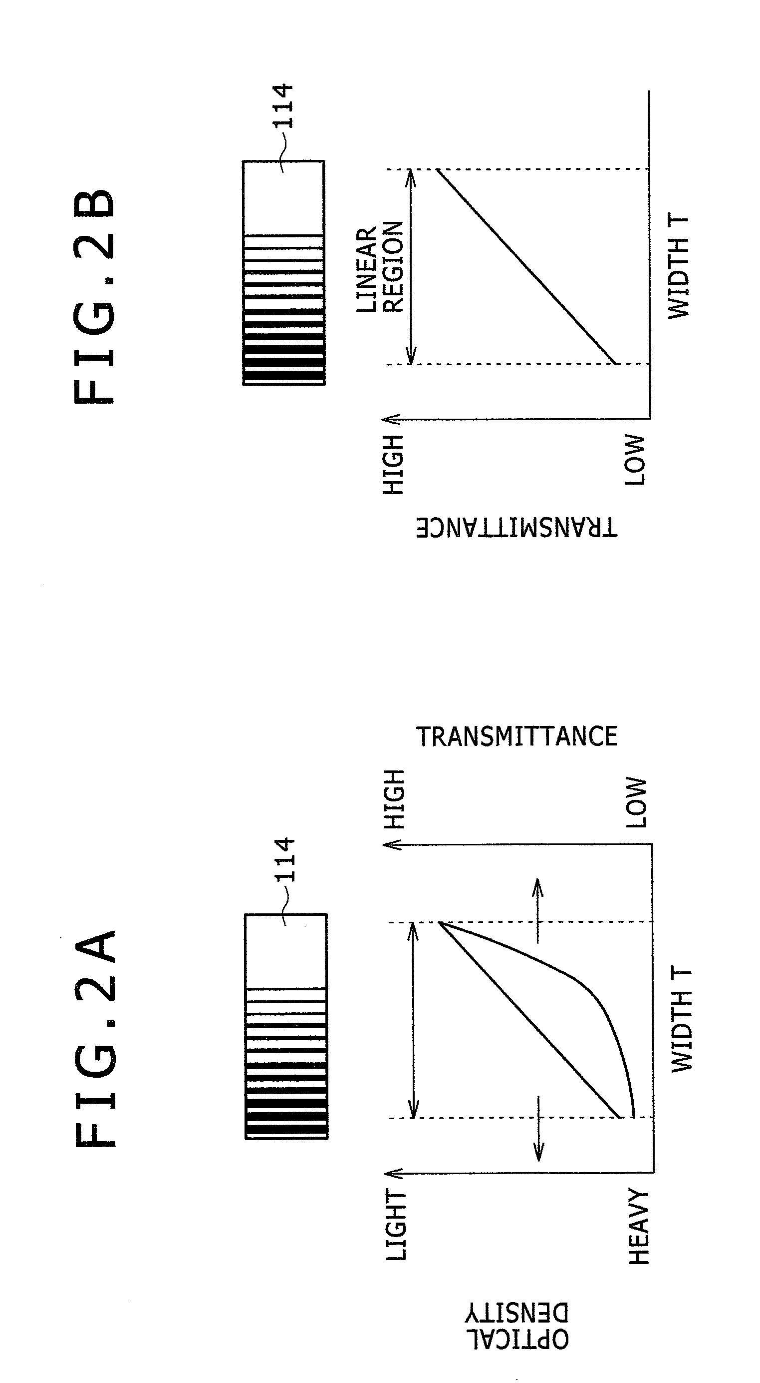
[0040]FIG. 1 illustrates a surface defect inspecting apparatus having a defect detection optical system and defect-detected image processing, which includes an irradiation optical system 200 that irradiates a light beam on a surface of a face plate of a disk 1 mounted on a stage 500 to scan the surface of the face plate, a light-receiving optical system 300 having shading filters 111 and 114 with shading differences causing an amount of specular reflection light from the face plate resulting from the light beam irradiated on the disk 1 to be changed and receiving the specular reflection light that has transmitted the shading filters, and a processing unit 400 that identifies defects on the surface of the face plate from the change in amount of specular reflection light that has transmitted the shading filters. Hereinafter, details of the respective constitutional components will be described with respective operations.

[0041]In the irradiation optical system 200, a laser beam output ...


PUM

PropertyMeasurementUnit
transmittanceaaaaaaaaaa

Abstract

There is provided a defect inspecting apparatus, which includes an irradiating optical system of irradiating a light beam on a surface of a face plate of a disk mounted on a stage to scan the surface of the face plate, a light-receiving optical system of receiving specular reflection light that has transmitted a shading filter with a shading difference that changes an amount of the specular reflection light from the face plate resulting from the light beam irradiated on the disk, and a processing unit of identifying defects on the surface of the face plate from the change in amount of the specular reflection light that has transmitted a filter, so that a size and a height of the defect can be measured with high accuracy when irregular defects are determined, which is not easily achieved by a conventional lens effect.

Description

CLAIM OF PRIORITY[0001]The present application claims priority from Japanese Patent Application JP 2007-316524 filed on Dec. 7, 2007, the content of which is hereby incorporated by reference into this application.FIELD OF THE INVENTION[0002]The present invention relates to a surface defect inspecting apparatus, and in particular, to a surface defect inspecting apparatus of a face plate such as a magnetic disk or its aluminum plate (i.e., an aluminum substrate) or a glass plate (i.e., a glass substrate), which can detect with high accuracy the size of a concave defect or a convex defect on the surface of the face plate and can further detect with high accuracy the size and the depth or the size and the height, of an irregular defect on the surface of the face plate.DESCRIPTION OF THE RELATED ART[0003]A technique of detecting with high accuracy the concave defects and the convex defect is disclosed in JP-A-Hei13 (2001)-174415, wherein a light receiver has a sensor array composed of pl...

Claims


Application Information

Patent Timeline
Patent Type & Authority Patents(United States)
IPC IPC(8): G01N21/00G01N21/88G01N21/95
CPCG01B11/022G01B11/0608G01B11/285G01N21/88G01N2021/8887
Inventor HARIYAMA, TATSUOYOSHIDASERIKAWA, SHIGERU
Owner HITACHI HIGH-TECH CORP
Why Eureka
Try Eureka