
Resistance change memory device

a memory device and resistance change technology, applied in the direction of information storage, static storage, digital storage, etc., can solve the problems of non-stable resistance change, significant increase in the number of waiting cells, and non-negligible enhancement of leakage curren

Active Publication Date: 2011-09-20
KIOXIA CORP
View PDF21 Cites 26 Cited by
  • Summary
  • Abstract
  • Description
  • Claims
  • Application Information

AI Technical Summary

Benefits of technology

This configuration enables faster and more efficient data transfer while maintaining stability in resistance changes, enhancing the capacity and performance of resistance change memory devices beyond traditional NAND-type flash memory.

Problems solved by technology

However, variable resistance elements (resistance change material) that are used as the storage layers of memory cells may have such characteristics that they would not exhibit stable resistance change unless a high voltage is applied thereto.
In addition, given that the large capacity file memory is achieved through configuration of cell arrays in a three-dimensional manner, there will be a non-negligible enhancement in leakage current when diodes used as access elements of memory cells are reverse-biased, in addition to a significant increase in the number of waiting cells.

Method used


Image

  • Resistance change memory device
  • Resistance change memory device
  • Resistance change memory device

Examples


Embodiment Construction

[0078]A brief overview of embodiments of the present invention follows.

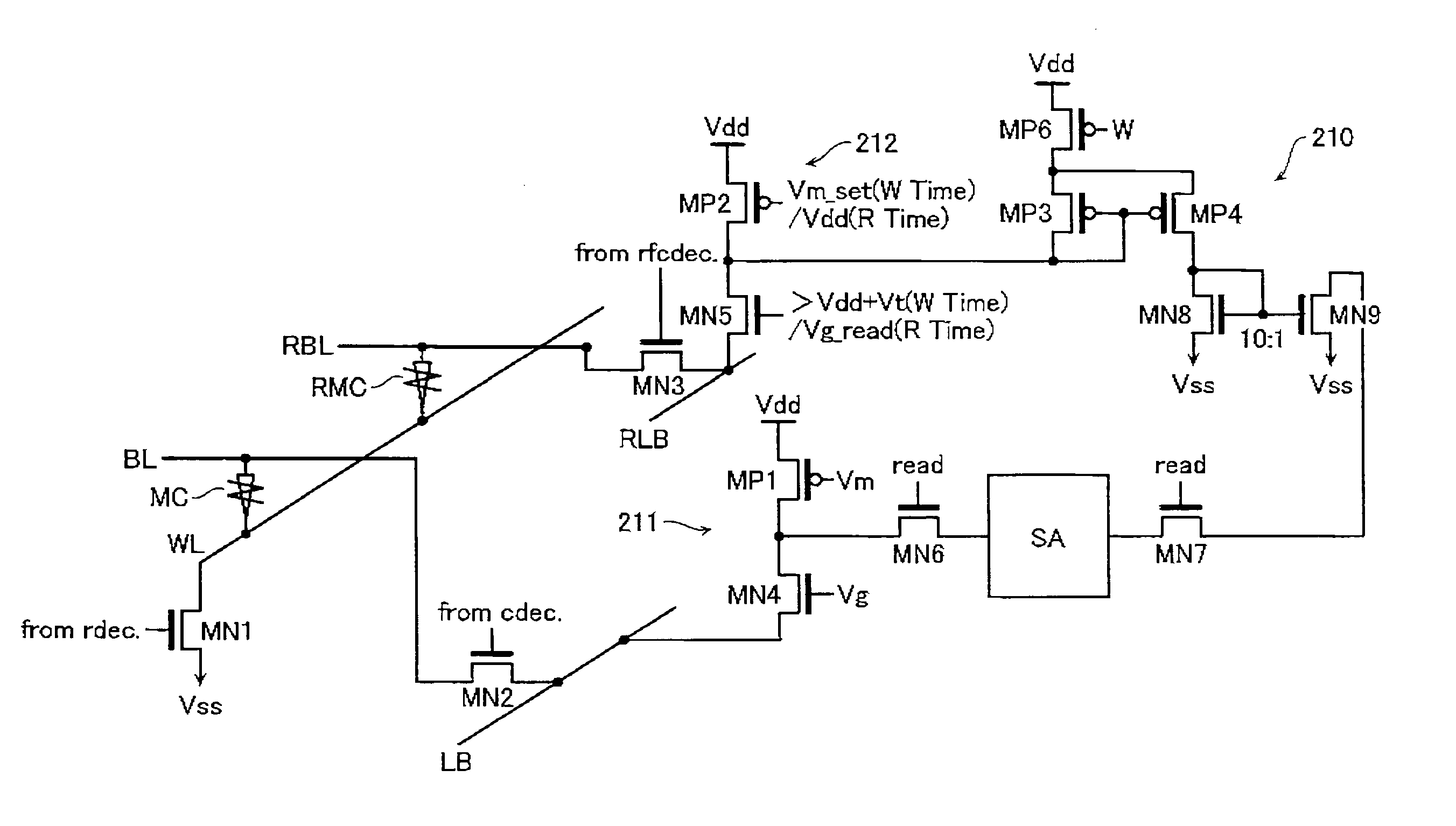
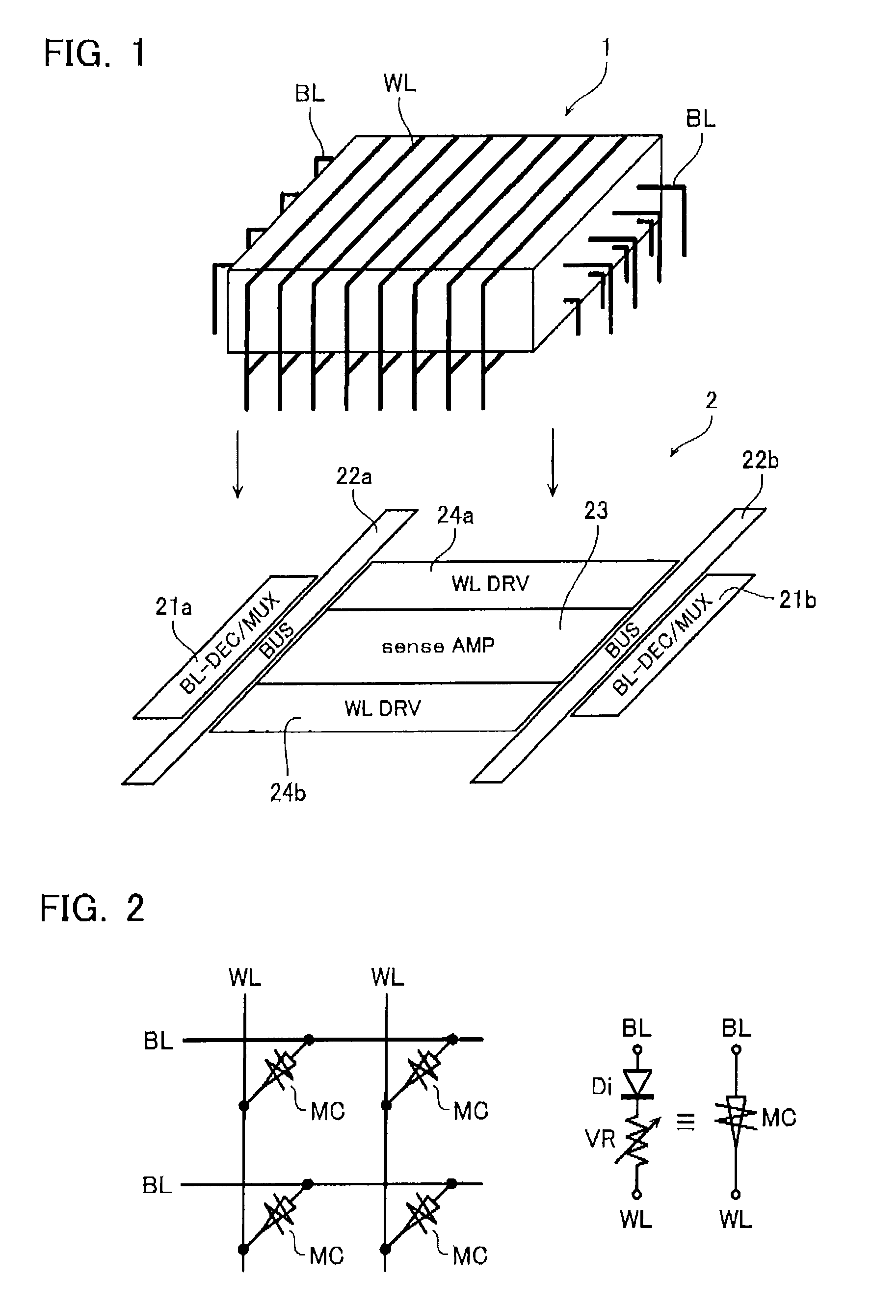
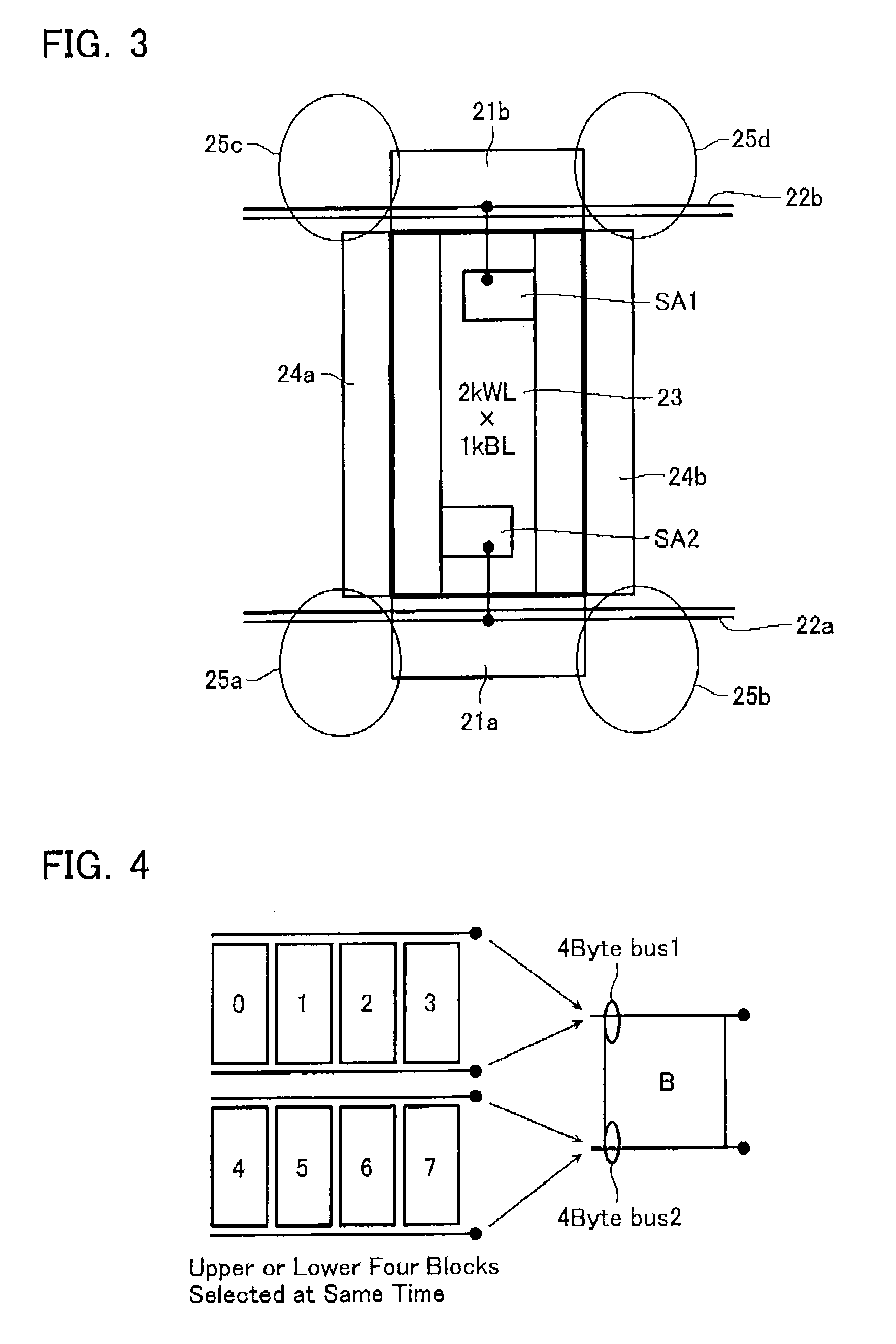
[0079]To provide a large capacity file memory, such a cell array is used where resistance change type memory cells are arranged in a three-dimensional manner. Preferably, the cell array involves a three-dimensional cell array block as a unit, and such three-dimensional cell array blocks are further arranged in a two-dimensional manner.

[0080]As an initial setting operation for stabilizing the state of resistance change type memory cells, a forming operation is performed to set the memory cells at a certain resistance state, e.g., a low resistance state (set state) by applying a certain voltage.

[0081]To perform data sensing with less effects of leakage current, when a word line and a bit line are selected in a mat of a cell array block, a reference bit line is selected at the same time that is driven by the same word line and connected to a reference cell on the same layer. The data sensing is performed through cel...


PUM


Abstract

A resistance change memory device includes a cell array having multiple layers of mats laminated thereon, each of the mats having word lines and bit lines intersecting each other as well as resistance change type memory cells arranged at intersections thereof, each of the mats further having therein a reference cell and a reference bit line connected to the reference cell, the reference cell set to a state of a certain resistance value; a selection circuit configured to select a word line in each mat of the cell array, and select a bit line intersecting a selected word line and the reference bit line at the same time; and a sense amplifier configured to sense data by comparing respective cell currents of a selected memory cell on the selected bit line and the reference cell on the reference bit line.

Description

CROSS REFERENCE TO RELATED APPLICATIONS[0001]This application is based on and claims the benefit of priority from prior Japanese Patent Application No. 2008-221620, filed on Aug. 29, 2008, the entire contents of which are incorporated herein by reference.BACKGROUND OF THE INVENTION[0002]1. Field of the Invention[0003]The present invention relates to a resistance change memory device, and in particular, to a memory device having cell array blocks, each including memory cells arranged in a three-dimensional manner.[0004]2. Description of the Related Art[0005]Resistive memory (Resistance RAM; ReRAM), which changes the resistance state of material with voltage, current, heat, etc., and utilizes the resistance state as data, has gained increasing attention as a likely candidate for replacing NAND-type flash memory (see, for example, Y. Hosoi et al, “High Speed Unipolar Switching Resistance RAM (RRAM) Technology” IEEE International Electron Devices Meeting 2006 Technical Digest p. 793-796...

Claims


Application Information

Patent Timeline
Patent Type & Authority Patents(United States)
IPC IPC(8): G11C11/00
CPCG11C8/12G11C13/00G11C13/004G11C13/0069G11C2013/0054G11C2013/009G11C2213/71G11C2213/72
Inventor TODA, HARUKI
Owner KIOXIA CORP
Learn More