Substrate cleaning device and substrate cleaning method

a cleaning device and substrate technology, applied in the direction of cleaning process and apparatus, cleaning liquids, chemistry apparatus and processes, etc., can solve the problems of increasing the possibility of water drops remaining on the protective film, water drops or watermarks affecting the resolution of parts of the circuit pattern underlying water drops or watermarks, and cleaning liquid film breaks, so as to achieve the effect of quick completion of the cleaning process

Inactive Publication Date: 2011-10-18
TOKYO ELECTRON LTD
View PDF16 Cites 5 Cited by
  • Summary
  • Abstract
  • Description
  • Claims
  • Application Information

AI Technical Summary

Benefits of technology

[0016]The present invention has been made under such circumstances and it is therefore an object of the present invention to provide a substrate cleaning device and a substrate cleaning method capable of cleaning a substrate by a spin-cleaning process and of drying the substrate so that any water drops may not remain on the substrate or so that water drops remaining on the substrate may be reduced.
[0026]According to the present invention, the region onto which the cleaning liquid is poured is moved from the central part toward the circumference of the substrate and the gas is jetted at a region behind the region onto which the cleaning liquid is poured with respect to the rotating direction of the substrate. Consequently, the gas jetted at the substrate exerts an outward force on a liquid film of the cleaning liquid poured onto the substrate and the cleaning liquid flowing in a circumferential direction is caused to flow outward. Therefore, a dry region in a surface of the substrate expands rapidly outward even if the substrate is rotated at a low rotating speed that will not cause the cleaning liquid run wildly, the cleaning liquid will not stagnate at a radial position, drops of the cleaning liquid can be surely removed and a cleaning process can be quickly completed.
[0027]According to the present invention, the flow of the cleaning liquid poured through the cleaning liquid pouring nozzle onto the surface of the substrate is restrained from flowing by the liquid damming member disposed at a height equal to or lower than the height of the nozzle exit of the liquid pouring nozzle. Consequently, the cleaning liquid collects in a large mass near the liquid damming member and an increased centrifugal force acts radially outward on the cleaning liquid, the cleaning liquid will not stagnate at a radial position, drops of the cleaning liquid can be surely removed and a cleaning process can be quickly completed.

Problems solved by technology

The possibility that the wafer wetted with water drops is carried from an exposure system to a coating and developing system is a problem in the immersion exposure method.
If the wafer W is wetted with water drops or if water drops have dried and watermarks are formed on the wafer W in the heat treatment, the water drops or the watermarks affect adversely to the resolution of parts of the circuit pattern underlying the water drops or the watermarks.
However, the following problems arise in cleaning the wafer processed by the immersion exposure process.
However, the high repellency of the protective film increases the possibility of water drops remaining on the protective film.
Consequently, a cleaning liquid film breaks and cleaning liquid drops cannot be easily removed, i.e., cleaning liquid drops do not roll radially outward on the wafer W. Consequently, the cleaning liquid drops cannot be completely removed even if the parameters are adjusted.
Therefore, the nozzle 14 unavoidably needs to be moved at a low moving speed and processing speed is unavoidably low.
The adjustment of the process parameters of the known spin cleaning process is difficult when the wafer is rotated at a high rotating speed.
The adjustment of the process parameters becomes more difficult when the protective film is formed on the wafer because it is expected that different device makers use different types of protective films and contact angle between the protective film and the cleaning liquid changes with time.
On the other hand, the cleaning process takes a long time and there is strong possibility of water drops remaining on the wafer when the wafer is rotated at a low rotating speed.
If water drops exist on the surface of the substrate, the so-called water marks, namely, dehydrated stains, will be formed on the surface of the substrate before the substrate is transferred to the exposure unit and will cause defects during an exposure process.

Method used


Image

  • Substrate cleaning device and substrate cleaning method
  • Substrate cleaning device and substrate cleaning method
  • Substrate cleaning device and substrate cleaning method

Examples


Embodiment Construction

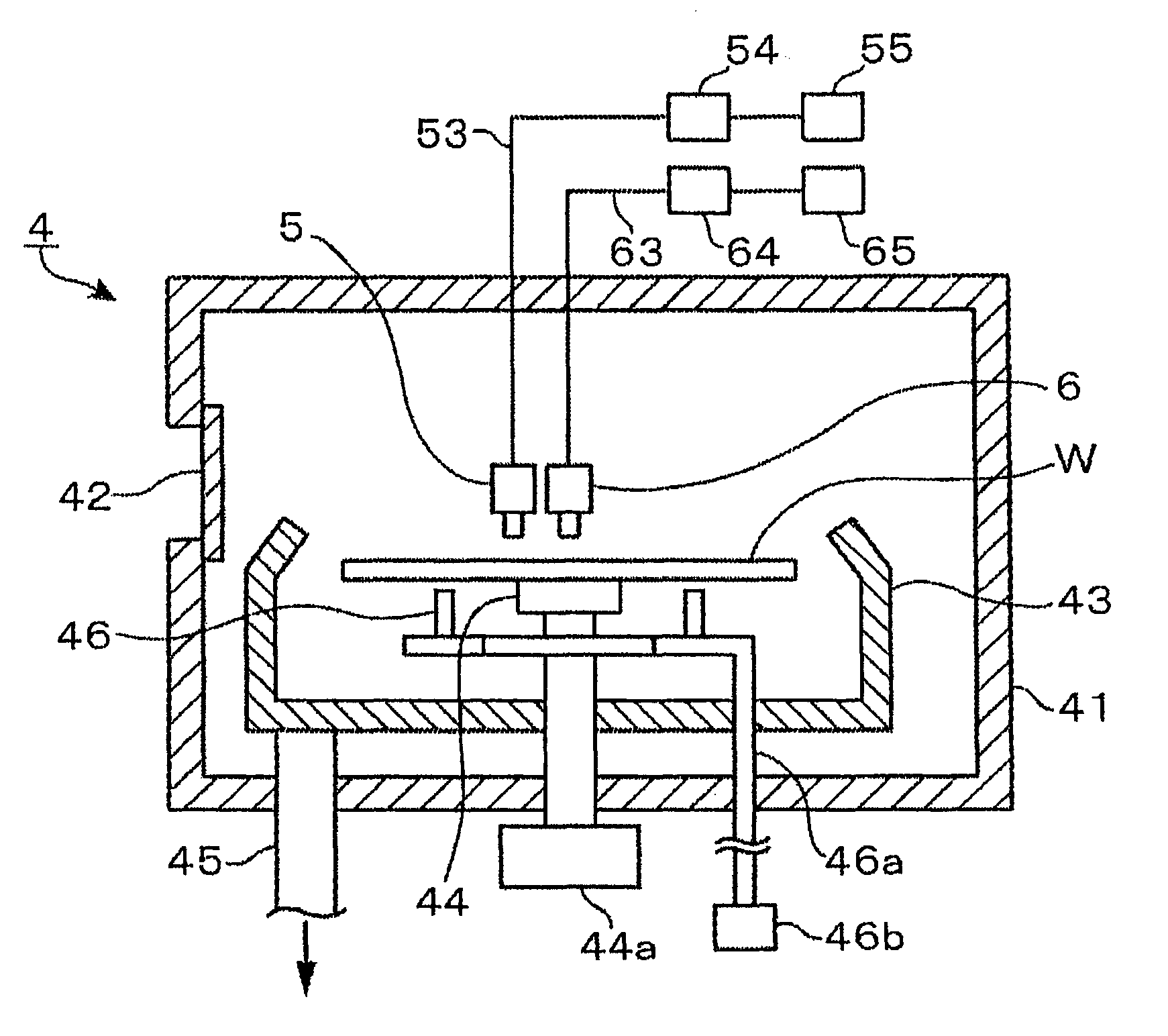
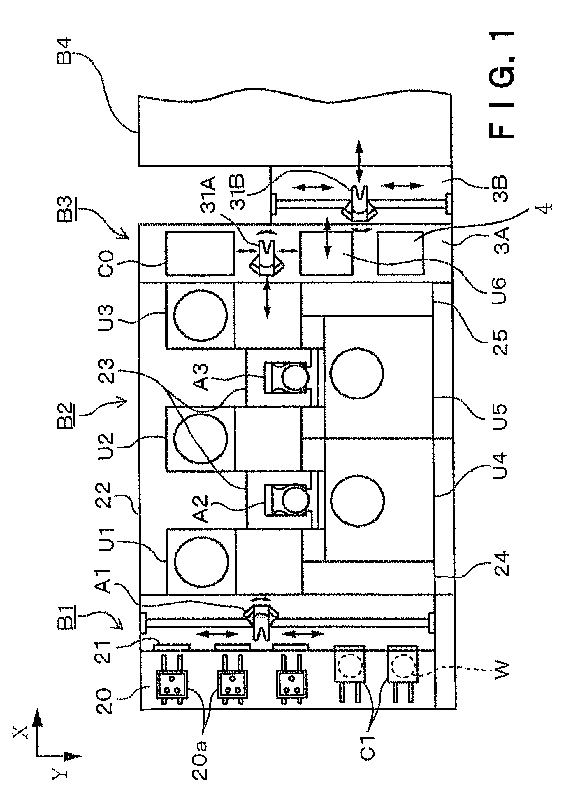
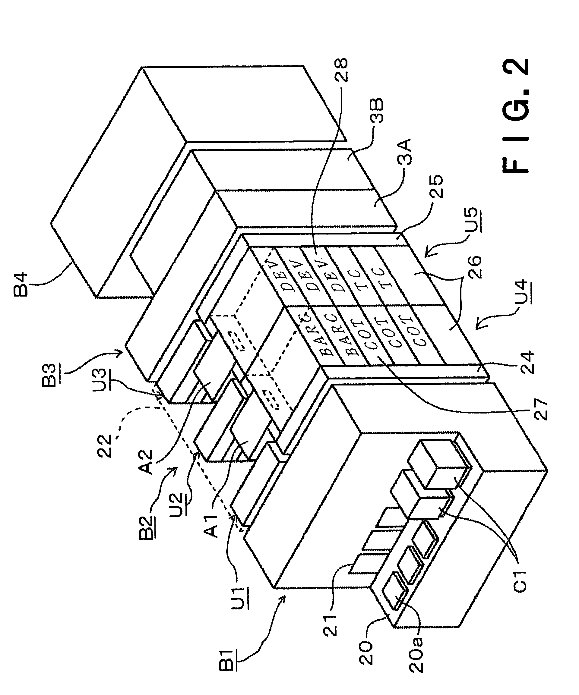
[0046]A substrate cleaning device in a preferred embodiment according to the present invention will be briefly described with reference to FIGS. 1 and 2 as applied to an immersion exposure system. The immersion exposure system is built by connecting an exposure system to a coating and developing system. Referring to FIGS. 1 and 2, a carrier handling block B1 includes a carrier station 20 provided with carrier support tables 20a for supporting airtight carriers C1 thereon, respectively, gates 21 formed in a wall behind the carrier support table 20a, and a transfer device A1 capable of extending through the gate 21 to take out a wafer W from the carrier C1. The carrier C1 contains, for example, thirteen wafers W, namely, substrates.

[0047]A processing block B2 surrounded by a casing 22 is connected to the back end of the carrier handling block B1. The processing block B2 includes three shelf units U1, U2 and U3 each formed by stacking up heating and cooling systems in layers, liquid-pr...


PUM


Abstract

A substrate cleaning device and a substrate cleaning method reduces liquid drops remaining on a substrate to prevent the irregular heating of the substrate by a heating process due to liquid drops or water marks remaining on the substrate. A cleaning liquid is poured through a cleaning liquid pouring nozzle onto the surface of a substrate such that a region onto which the cleaning liquid is poured moves from a central part toward the circumference of the substrate. A gas is jetted radially outward at a region on the surface of the substrate behind a region onto which the cleaning liquid is poured with respect to the rotating direction of the substrate. The gas forces a liquid film of the cleaning liquid flowing on the surface of the substrate to flow in a circumferential direction and a radially outward direction.

Description

BACKGROUND OF THE INVENTION[0001]1. Field of the Invention[0002]The present invention relates to a substrate cleaning device for cleaning a surface of a substrate processed by, for example, an emersion exposure process or a developing process, and a substrate cleaning method to be carried out by the substrate cleaning device.[0003]2. Description of the Related Art[0004]A photoresist pattern forming process, which is one of semiconductor device fabricating processes, coats a surface of a semiconductor wafer (hereinafter, referred to simply as “wafer”) with a resist film, exposes the resist film in a predetermined pattern, and develops the exposed resist film to form a resist pattern.[0005]Device patterns have been progressively miniaturized and the thickness of films shows a trend to decrease in recent years. Consequently, there has been a growing request for higher exposure resolution. To improve exposure resolution, efforts have been made to develop exposure techniques, such as an ...

Claims


Application Information

Patent Timeline
Patent Type & Authority Patents(United States)
IPC IPC(8): B08B3/00
CPCH01L21/67051H01L21/304
Inventor YAMAMOTO, TAROKYOUDA, HIDEHARUKAWASAKI, TETSUSHIMURA, SATORU
Owner TOKYO ELECTRON LTD
Why Eureka
Try Eureka