
Liquid crystal display device having column spacers and first auxiliary spacers that include a plurality of spaced apart patterns

a liquid crystal display and column spacer technology, applied in non-linear optics, instruments, optics, etc., can solve the problems of reducing the quality of liquid crystal cell images, incorrect operation, and increasing the use of the seal dispenser method, so as to prevent the wrong working of the gate driver, prevent electrical shorts, and reduce the output of the gate-driving signal

Active Publication Date: 2011-10-25
LG DISPLAY CO LTD
View PDF18 Cites 4 Cited by
  • Summary
  • Abstract
  • Description
  • Claims
  • Application Information

AI Technical Summary

Benefits of technology

[0023]An object of embodiments of the invention is to provide a liquid crystal display device and a method of manufacturing the same that prevent wrong working of a gate driver due to a parasitic capacitance between thin film transistors of the gate driver and a common electrode in a gate-in-panel (GIP) type.
[0024]Another object of embodiments of the invention is to provide a liquid crystal display device and a method of manufacturing the same that prevent electrical short due to particles going to the gate driver.
[0025]Another object of embodiments of the invention is to provide a liquid crystal display device and a method of manufacturing the same that solve a problem of lowering output of gate-driving signals due to line delay of the gate driver and a signal line connected to the gate driver.

Problems solved by technology

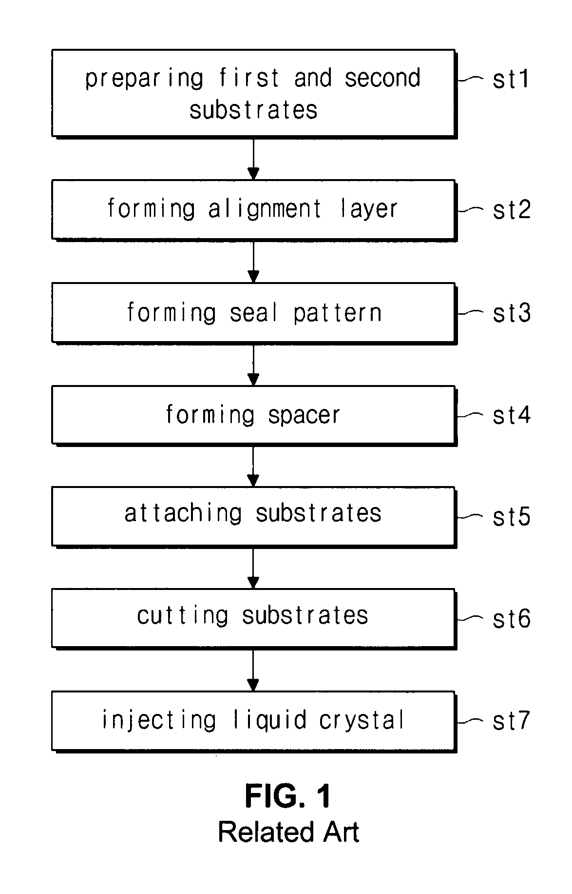
However, since the screen mask is not suitable for a wide substrate and a contamination by contact between the mask and the alignment layer often occurs, use of the seal dispenser method has gradually increased.
If the substrates are attached beyond the margin, there is leakage of light, to thereby decrease the quality of images of the liquid crystal cell.
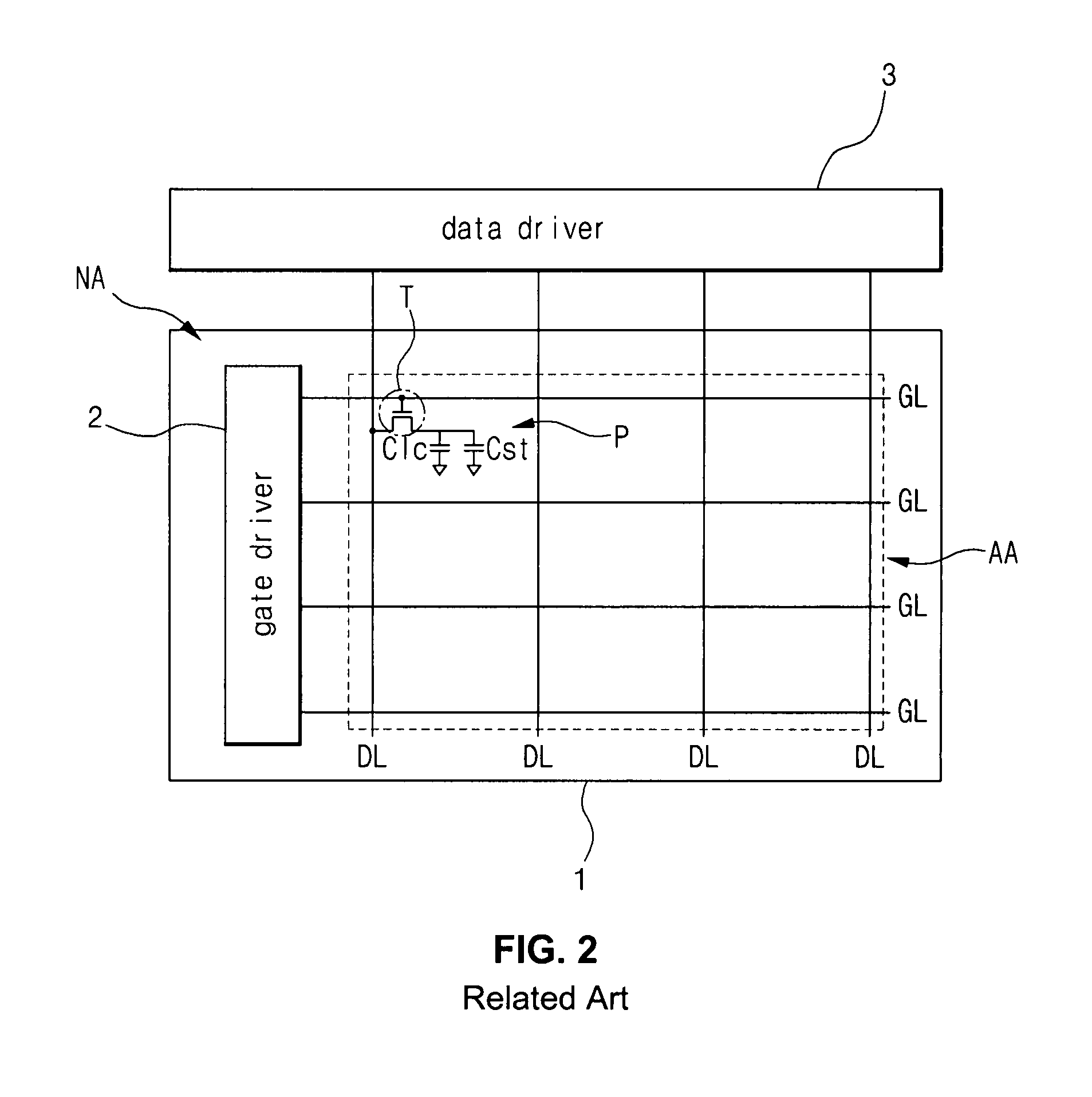
The parasitic capacitance lowers characteristics of the thin film transistor and affects the gate-driving signals Vout1 to VoutN to thereby cause incorrect operation.

Method used


Image

  • Liquid crystal display device having column spacers and first auxiliary spacers that include a plurality of spaced apart patterns
  • Liquid crystal display device having column spacers and first auxiliary spacers that include a plurality of spaced apart patterns
  • Liquid crystal display device having column spacers and first auxiliary spacers that include a plurality of spaced apart patterns

Examples


first embodiment

[0045]FIG. 4 is a schematic plan view illustrating a liquid crystal panel for a liquid crystal display (LCD) device according to the invention. As shown in FIG. 4, a liquid crystal panel 100 includes a first substrate 102 and a second substrate 104. A display area AA for displaying images and a non-display area NA surrounding the display area AA are defined in the first and second substrates 102 and 104. Column spacers 204 are disposed in the display area AA and are spaced apart from each other with a certain distance. The column spacers 204 keep a cell gap uniform. The column spacers 204 are formed through a photolithographic process patterning a thin film using a photosensitive material, such as photoresist. The column spacers 204 may be formed on the second substrate 104. Acrylic organic materials are used as a material for the column spacers 204. The column spacers 204 may be formed by directly exposing and developing a photosensitive organic material without using photoresist. ...

second embodiment

[0055]As shown in FIG. 7 and FIG. 8, the liquid crystal panel 400 of the second embodiment includes first and second substrates 402 and 404 that overlap each other. A display area AA and a non-display area NA are defined on the first and second substrates 402 and 404. The display area AA displays images, and the non-display area NA surrounds the display area AA. Although not shown in the figures, gate lines and data lines cross one another to define pixel regions on an inner surface of the first substrate 402. A thin film transistor is disposed at each crossing portion of the gate and data lines. A pixel electrode is disposed in each pixel region and is connected to the thin film transistor. A storage capacitor may be formed in the pixel region and may be connected to the pixel electrode.

[0056]A black matrix (not shown), a color filter layer (not shown) and a common electrode 406 are formed on an inner surface of the second substrate 404 in the display area AA. The common electrode ...

third embodiment

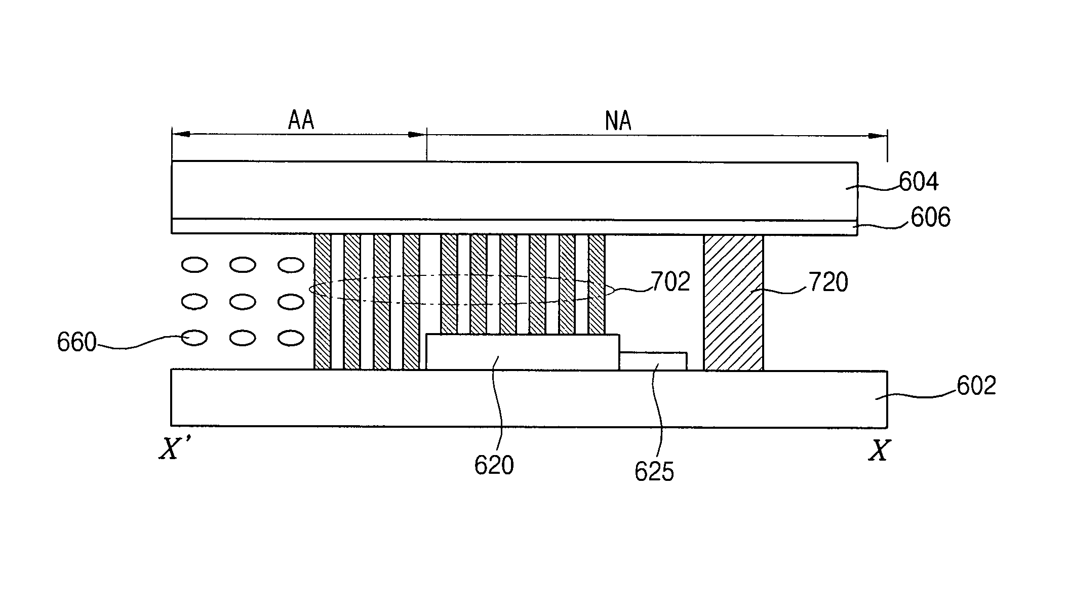
[0066]In FIG. 9 and FIG. 10, the liquid crystal panel 600 of the third embodiment includes first and second substrates 602 and 604 that overlap each other. A display area AA and a non-display area NA are defined on the first and second substrates 602 and 604. The display area AA displays images, and the non-display area NA surrounds the display area AA.

[0067]Column spacers 704 are formed in the display area AA between the first and second substrates 602 and 604 and correspond to regions except for pixel regions. The column spacers 704 keep a distance between the first and second substrates 602 and 604 uniform.

[0068]A seal pattern 720 is formed in the non-display area NA and surrounds the display area AA. The seal pattern 720 may include conductive ball spacers therein. A gate driver 620 and a signal line 625 for the gate driver 620 are formed in the non-display area NA. The gate driver 620 and the signal line 625 are disposed inside the seal pattern 720.

[0069]A first auxiliary space...


PUM

PropertyMeasurementUnit
areaaaaaaaaaaa
parasitic capacitanceaaaaaaaaaa
distanceaaaaaaaaaa

Abstract

A liquid crystal display device includes first and second substrates spaced apart from each other, on which a display area and a non-display area are defined, a liquid crystal layer interposed between the first and second substrates, a seal pattern in the non-display area between the first and second substrates, a driver in the non-display area on the first substrate, column spacers in the display area between the first and second substrates, and a first auxiliary spacer between the driver and the second substrate.

Description

[0001]The invention claims the benefit of Korean Patent Application Nos. 10-2006-0138872 filed in Korea on Dec. 29, 2006 and 10-2007-0039311, filed in Korea on Apr. 23, 2007, which are hereby incorporated by reference in their entirety.BACKGROUND OF THE INVENTION[0002]1. Field of the Invention[0003]Embodiments of the invention relate to a display device, and more particularly, to a liquid crystal display device and a method of manufacturing the same. Although embodiments of the invention are suitable for a wide scope of applications, it is particularly suitable for preventing signal delay within a gate driver and gate lines for a gate-in-panel (GIP) type.[0004]2. Discussion of the Related Art[0005]Generally, liquid crystal display (LCD) devices, as flat panel display devices, change arrangement of liquid crystal molecules, which are initially arranged along a predetermined direction, by applying an electric field to the liquid crystal molecules to control transmittance of light pass...

Claims


Application Information

Patent Timeline
Patent Type & Authority Patents(United States)
IPC IPC(8): G02F1/1339G02F1/1343
CPCG02F1/13394G02F2001/133388G02F2001/13396G02F1/133388G02F1/13396G02F1/1339
Inventor KIM, HONG-JAEKIM, TAE-MANKWON, KEUK-SANG
Owner LG DISPLAY CO LTD
Learn More