Product setup sharing for multiple inspection systems

a technology of multiple inspection systems and product setups, applied in the field of product setup sharing, can solve the problems of large variation between systems, inability to use tools, and inability to match tools,

Active Publication Date: 2011-10-25
ONTO INNOVATION INC
View PDF57 Cites 16 Cited by
  • Summary
  • Abstract
  • Description
  • Claims
  • Application Information

AI Technical Summary

Problems solved by technology

However, this often results in large variations between systems.
Furthermore, optics in each system have unique distortions and light transmission efficiencies that are field of view dependent.
The result is that tool to tool correlation is in many cases unacceptable to the user.

Method used


Image

  • Product setup sharing for multiple inspection systems
  • Product setup sharing for multiple inspection systems
  • Product setup sharing for multiple inspection systems

Examples


Embodiment Construction

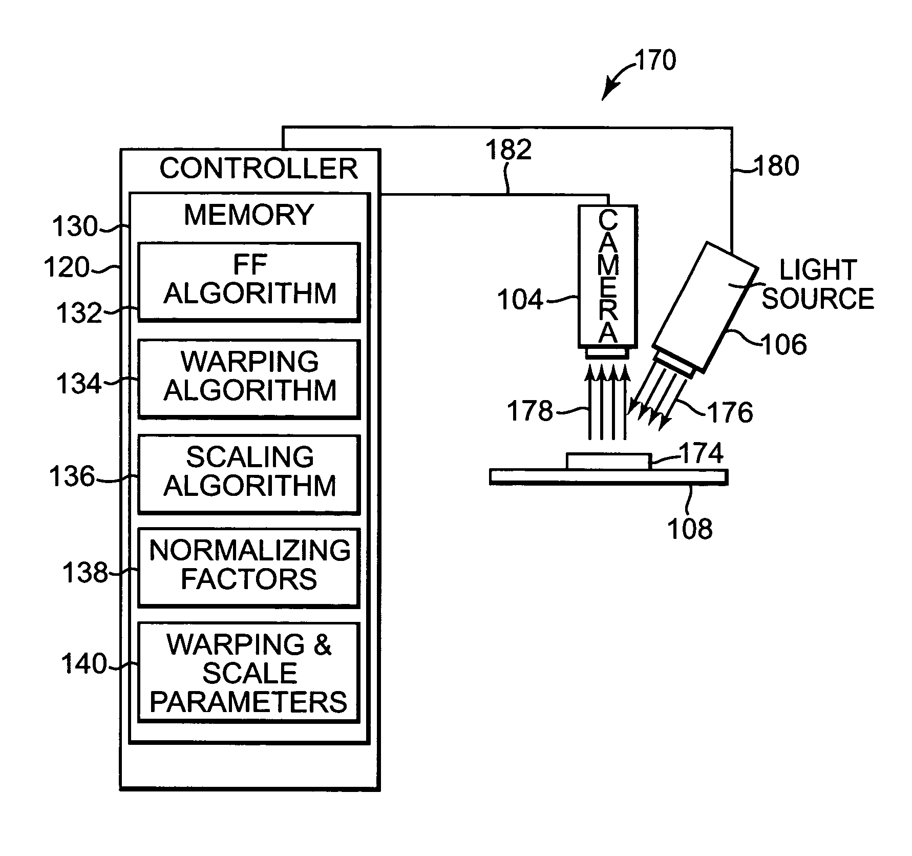
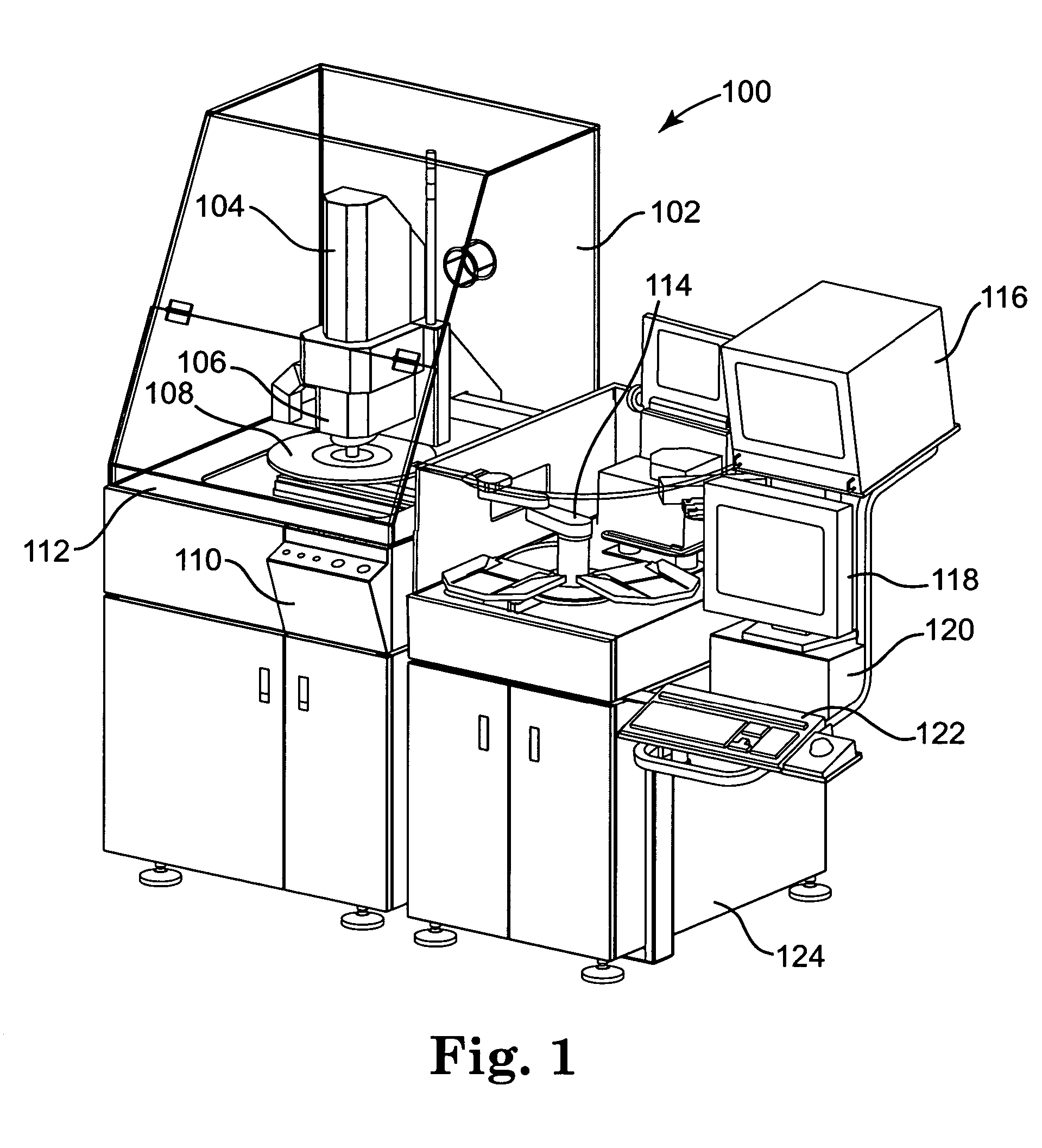
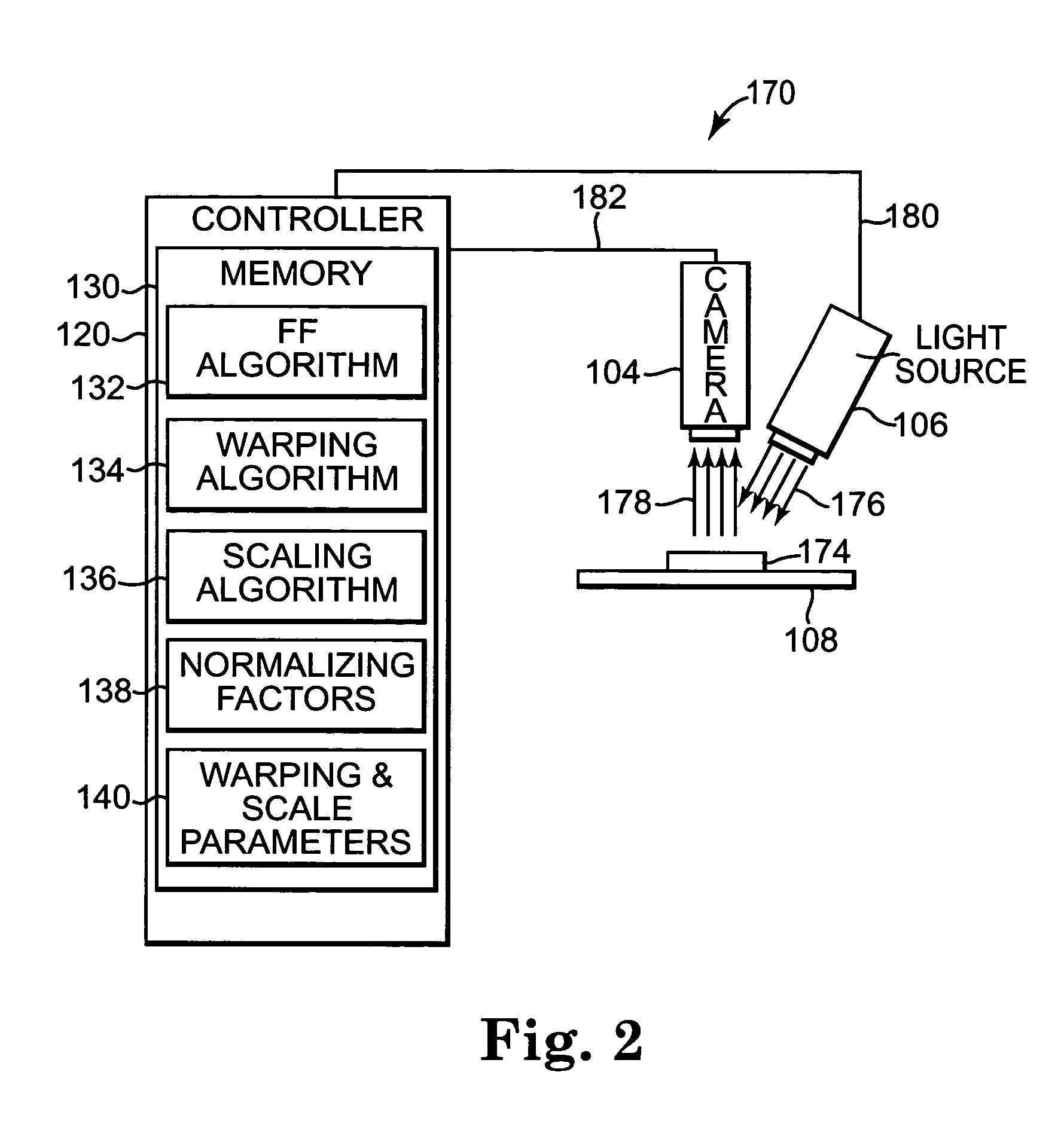
FIG. 1 is a diagram illustrating one embodiment of a semiconductor inspection system 100. Semiconductor inspection system 100 includes a hood 102, a camera 104, an inspection light source 106, a wafer test plate 108, a wafer alignment device 112, a control panel 110, a robot 114, a display 116, a system parameters display 118, a computer system or controller 120, a parameter input device 122, and a frame 124. In one embodiment, semiconductor inspection system 100 is an automated system that is configured to inspect substrates, such as semiconductor wafers and semiconductor die.

Camera 104 is used for visual inputting of good die during training and for visual inspection of other unknown quality die during inspection. The camera may be any type of camera capable of high resolution inspection. An example of such a camera is a charge-coupled device (CCD) inspection camera used to capture die or other images during defect analysis. In one embodiment, camera 104 is a high resolution CCD c...


PUM

PropertyMeasurementUnit
optical image warpingaaaaaaaaaa
optical image scale correctionaaaaaaaaaa
optical imageaaaaaaaaaa

Abstract

An inspection tool includes a camera for obtaining images of a wafer and a controller configured for performing light source flat field correction, optical image warping correction, and optical image scale correction of the images. In operation, separate inspection tools are calibrated separately to obtain a characteristic response with respect to imaging and / or illumination for each such inspection tool. A standard target is then imaged by each inspection tool and the response of each of the inspection tools is normalized to ensure uniformity of the output of each inspection tool with respect to the other inspection tools.

Description

BACKGROUND1. Technical FieldThe present invention relates to product setup sharing prior to and during inspection.2. Background InformationOver the past several decades, the semiconductor has exponentially grown in use and popularity. The semiconductor has in effect revolutionized society by introducing computers, electronic advances, and generally revolutionizing many previously difficult, expensive and / or time consuming mechanical processes into simplistic and quick electronic processes. This boom in semiconductors has been fueled by an insatiable desire by business and individuals for computers and electronics, and more particularly, faster, more advanced computers and electronics whether it be on an assembly line, on test equipment in a lab, on the personal computer at one's desk, or in the home electronics and toys.The manufacturers of semiconductors have made vast improvements in end product quality, speed and performance as well as in manufacturing process quality, speed and ...

Claims


Application Information

Patent Timeline
Patent Type & Authority Patents(United States)
IPC IPC(8): G06K9/00G06T5/00
CPCG06T5/006G06T5/008Y10T29/49131G06T2207/30148
Inventor WATKINS, CORYSIMPKINS, PATRICK
Owner ONTO INNOVATION INC
Why Eureka
Try Eureka