Supercharge Your Innovation With Domain-Expert AI Agents!

Electron emission device

a technology of electron emission device and light source, which is applied in the manufacture of electrode systems, electric discharge tubes/lamps, and discharge tubes luminescnet screens, etc., can solve the problems of high cost, considerable energy loss, and both aforementioned light emission devices, and achieve the effect of reducing the thickness of the electron emission devi

Inactive Publication Date: 2011-11-01
IND TECH RES INST
View PDF14 Cites 0 Cited by
  • Summary
  • Abstract
  • Description
  • Claims
  • Application Information

AI Technical Summary

Benefits of technology

This solution improves light emitting uniformity, reduces device thickness, and lowers production costs by using a thin gas to induce electrons directly with the phosphor layer, minimizing energy loss and avoiding plasma generation, thus achieving high light emitting efficiency and simplified production.

Problems solved by technology

However, there are disadvantages in both aforementioned light emitting devices.
Moreover, the light emitting mechanism of gas discharge requires two processes to emit a visible light, thus, the energy loss is considerable, and it will cost more if plasma needs to be generated during the process.
In another aspect, electron emitter has to be evenly grown or disposed on the cathode of the field emission light source, however, the technology of mass-producing of such cathode structure is still immature, and the problems of poor electron emitter uniformity and poor production yield are still not resolved.
Moreover, the space between the cathode and the anode of field emission light source requires precise control, and ultra high vacuum packaging is difficult to process, so the cost of production increases accordingly.

Method used


Image

  • Electron emission device
  • Electron emission device
  • Electron emission device

Examples


Embodiment Construction

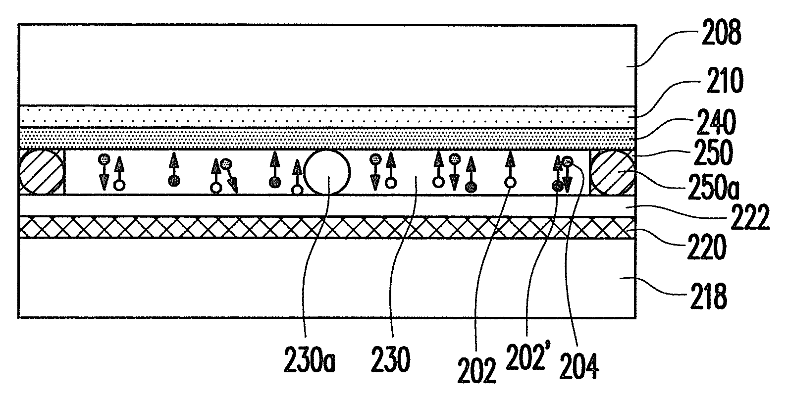
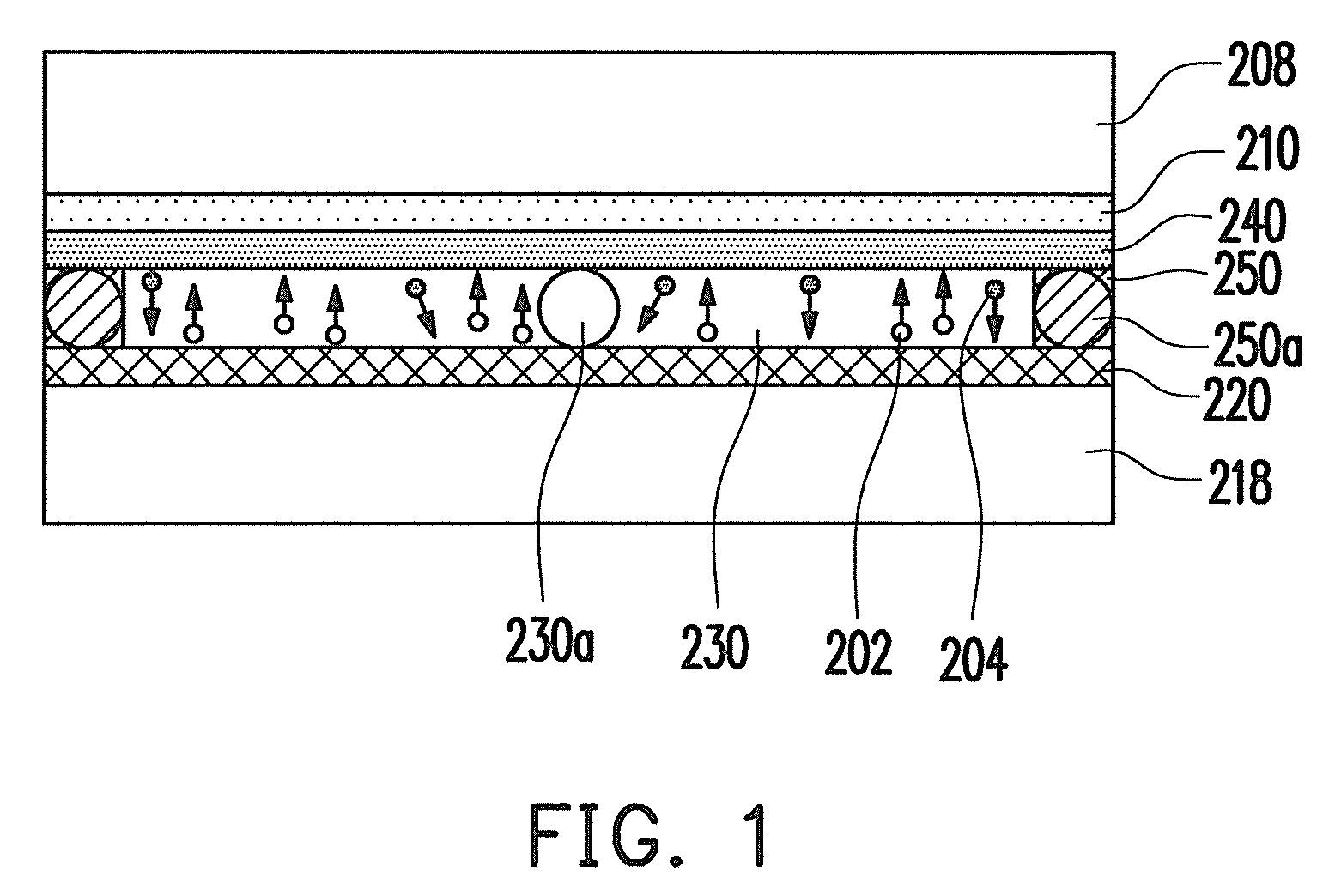
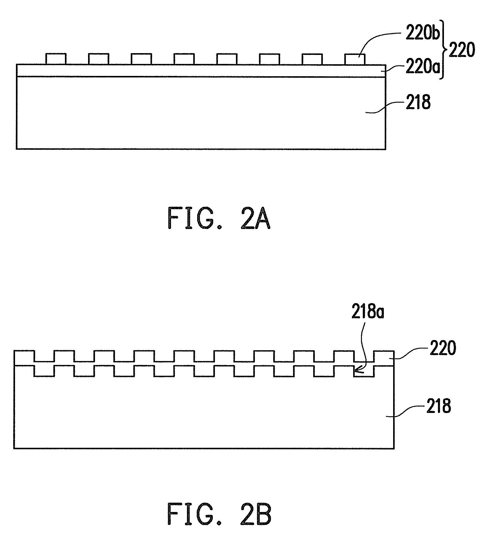
[0020]The electron emission device of the present invention has advantages of both the conventional gas discharge light source and the conventional field emission light source, and overcomes disadvantages of both aforementioned light emitting devices. To be specific, there is no need to form electron emitter in the electron emission device of the present invention; instead, electrons are induced easily from the cathode by using thin gas and react directly with the phosphor layer to emit light. Comparing with conventional gas discharge light source, the amount of the gas filled in the electron emission device of the present invention is enough when meeting the requirement of inducing electrons from the cathode. Since the UV light is not adopted in the present invention to irradiate the phosphor layer for emitting light, attenuation of materials in the device due to the UV irradiation is eliminated. According to experiments and theory, the gas is thin in electron emission device of th...


PUM


Abstract

An electron emission device including a first substrate, a second substrate, a gas, a sealant, and a phosphor layer is provided. The first substrate has a cathode thereon, and the cathode has a patterned profile. The second substrate is opposite to the first substrate and has an anode thereon. The sealant is disposed at edges of the first substrate and the second substrate to assemble the first and second substrates. The gas is disposed between the cathode and the anode and configured to induce a plurality of electrons from the cathode, wherein the pressure of the gas is between 10 torr and 10−3 torr. The phosphor layer is disposed on the moving path of the electrons to react with the electrons so as to emit light.

Description

CROSS-REFERENCE TO RELATED APPLICATION[0001]This application claims the priority benefit of Taiwan application serial no. 97147162, filed on Dec. 4, 2008. The entirety of the above-mentioned patent application is hereby incorporated by reference herein and made a part of specification.BACKGROUND OF THE INVENTION[0002]1. Field of the Invention[0003]The present invention relates to a light emitting device and a method of packaging the same. More particularly, the present invention relates to an electron emission device and a method of packaging the same.[0004]2. Description of Related Art[0005]Currently, light emitting devices applied in existing mass-produced include gas discharge light sources and field emission light sources. The gas discharge light source may be applied to a plasma panel or a gas discharge lamp, wherein gas that filled in a discharge chamber is dissociated under the effect of an electric field between a cathode and an anode, and due to gas conduction, transition o...

Claims


Application Information

Patent Timeline
Patent Type & Authority Patents(United States)
IPC IPC(8): H01J17/00
CPCH01J9/268H01J63/02
Inventor WANG, PO-HUNGLI, JUNG-YUCHEN, SHIH-PULIN, YI-PINGCHOU, YEN-ILIU, MING-CHUNG
Owner IND TECH RES INST
Features
  • R&D
  • Intellectual Property
  • Life Sciences
  • Materials
  • Tech Scout
  • Unparalleled Data Quality
  • Higher Quality Content
  • 60% Fewer Hallucinations
Learn More