
Integrated semiconductor optical device and optical apparatus using the same

a semiconductor optical device and optical apparatus technology, applied in semiconductor devices, semiconductor lasers, laser details, etc., can solve the problems of deteriorating device reliability, optical scattering loss, complex processes, etc., and achieve the effect of efficient injection and large band gap energy

Active Publication Date: 2011-11-22
SUMITOMO ELECTRIC IND LTD
View PDF5 Cites 5 Cited by
  • Summary
  • Abstract
  • Description
  • Claims
  • Application Information

AI Technical Summary

Benefits of technology

[0025]According to the above integrated semiconductor optical device, when carbon is used as a p-type dopant, diffusion of p-type dopant from the tunnel junction region to the active layer is reduced. This is because carbon has smaller diffusion coefficient than zinc that is commonly used as a p-type dopant. In addition, since carbon is doped to AlGaInAs at heavy doping concentration, an excellent tunnel junction is formed.
[0027]According to the above integrated semiconductor optical device, the first conductivity type semiconductor layer is composed of a GaInAsP layer, so that band gap energy of the n-type region of the tunnel junction region is reduced. In addition, light which propagates through the first active layer is prevented from being absorbed by the first conductivity type semiconductor layer of the tunnel junction region.
[0029]According to the above integrated semiconductor optical device, material of the second conductivity type semiconductor layer has larger band gap energy than that of the first conductivity type semiconductor layer, so that hole is efficiently injected.

Problems solved by technology

This discontinuity causes optical scattering loss.
In forming the isolation region, the number of processes of crystal growth increases, so that the processes are complicated.
However, since the ion implantation leads defect into the semiconducting crystal, it has been found out that when the isolation region is formed using the ion implantation, reliability of device deteriorates.

Method used


Image

  • Integrated semiconductor optical device and optical apparatus using the same
  • Integrated semiconductor optical device and optical apparatus using the same
  • Integrated semiconductor optical device and optical apparatus using the same

Examples


Embodiment Construction

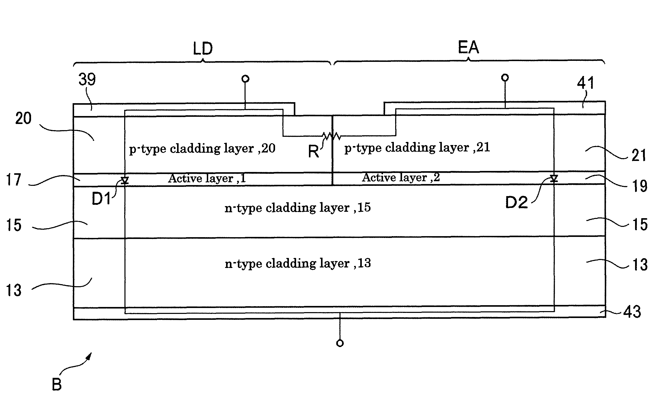
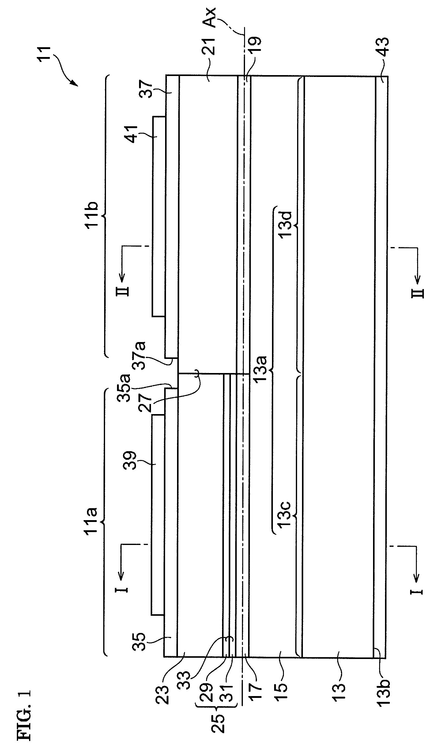
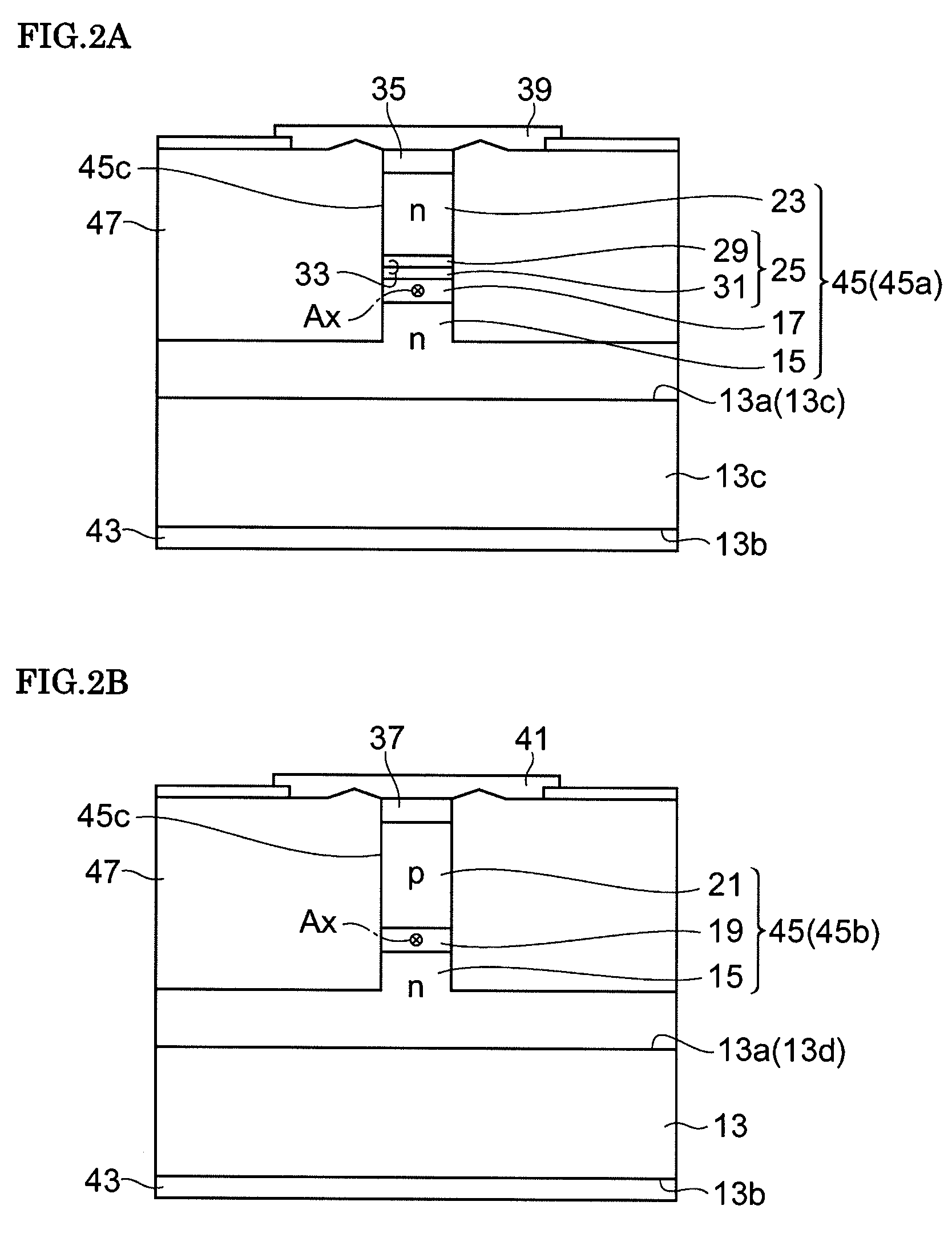
[0044]Findings of the present invention are easily understood by considering the following detailed description with reference to the accompanying drawings taken as an example. An embodiment of the integrated semiconductor optical device and the semiconductor optical apparatus according to the present invention will now be described with reference to the accompanying drawings. If available, the same reference numerals or signs are applied to the same elements.

[0045]FIG. 1 is a schematic view showing an integrated semiconductor optical device according to the present embodiment. The integrated semiconductor optical device 11 includes a first semiconductor optical device 11a and a second semiconductor optical device 11b. The integrated semiconductor optical device 11 includes a substrate 13, a first cladding layer 15, a first active layer 17, a second active layer 19, a second cladding layer 21, a third cladding layer 23 and a tunnel junction region 25. The substrate 13 has on the opp...


PUM


Abstract

In an integrated semiconductor optical device, a first cladding layer is made of a first conductivity type semiconductor. A first active layer for forming a first semiconductor optical device is provided on the first cladding layer in a first area of a principal surface of a substrate. A second active layer for forming a second semiconductor optical device is provided on the first cladding layer in a second area of the principal surface. A second cladding layer made of a second conductivity type semiconductor is provided on the second active layer. A third cladding layer made of a first conductivity type semiconductor is provided on the first active layer. A tunnel junction region is provided between the first active layer and the third cladding layer. The first active layer is coupled to the second active layer by butt joint. The second and third cladding layers form a p-n junction.

Description

BACKGROUND OF THE INVENTION[0001]1. Field of the Invention[0002]The present invention relates to an integrated semiconductor optical device and an optical apparatus using the same.[0003]2. Description of the Related Art[0004]Japanese Unexamined Patent Application Publication No. 64-28984 discloses an integrated semiconductor optical device. The integrated semiconductor optical device includes a distributed feedback laser diode (DFB laser diode), an optical modulator, and a connected portion provided between the DFB laser diode and the optical modulator. The connected portion is made of high-resistance semiconductor material.[0005]Japanese Unexamined Patent Application Publication No. 8-335745 discloses a semiconductor light emitting device. The semiconductor light emitting device includes a distributed feedback laser diode portion (or DFB laser diode portion), an optical modulator portion, and an isolation portion provided between the DFB laser diode portion and the optical modulato...

Claims


Application Information

Patent Timeline
Patent Type & Authority Patents(United States)
IPC IPC(8): H01L29/885H01L33/00
CPCH01S5/0265H01L29/885H01S5/3095
Inventor MURATA, MICHIO
Owner SUMITOMO ELECTRIC IND LTD
Learn More