Apparatus and method for testing of stacked die structure

a technology of integrated circuits and apparatuses, applied in the direction of measurement devices, instruments, semiconductor devices, etc., can solve the problems of cost saving, process taking significantly less time, and saving manufacturing tim

Active Publication Date: 2011-11-22
XILINX INC
View PDF19 Cites 52 Cited by
  • Summary
  • Abstract
  • Description
  • Claims
  • Application Information

AI Technical Summary

Benefits of technology

[0010]The method and apparatus of the present invention provide for testing of the base die and the stacked die without requiring configuration of the base die. Thereby, the testing process takes significantly less time than conventional processes that require configuration of the base die, saving manufacturing time and resulting in cost savings. These and other advantages of the present invention will become obvious to those of ordinary skill in the art after having read the following detailed description of the preferred embodiments, which are illustrated in the various drawings.

Problems solved by technology

Thereby, the testing process takes significantly less time than conventional processes that require configuration of the base die, saving manufacturing time and resulting in cost savings.

Method used


Image

  • Apparatus and method for testing of stacked die structure
  • Apparatus and method for testing of stacked die structure
  • Apparatus and method for testing of stacked die structure

Examples


Embodiment Construction

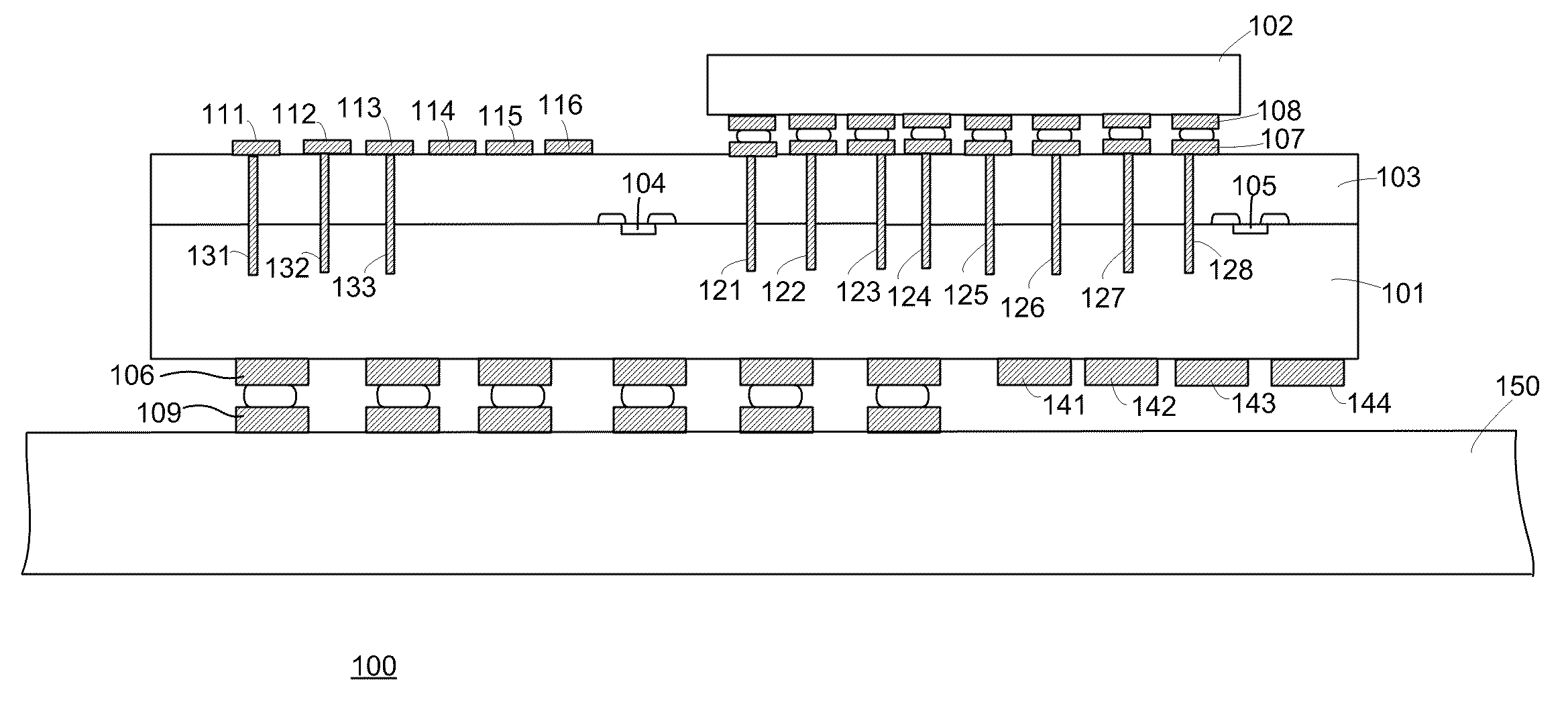
[0021]FIG. 1 shows an integrated circuit device 100 that includes a base die 101 and a stacked die 102 that is coupled to the back side of base die 101. Base die 101 includes a first set of contacts 107 that are formed the back side of base die 101 and a second set of contacts 106 that are formed on the face side of base die 101. In the present embodiment stacked die 102 is vertically stacked with base die 101, such that the face side of stacked die 102 is mounted to the back side of base die 101, with both of die 101-102 configured for face-down mounting in flip-chip fashion.

[0022]In one embodiment contacts 107 are a grid array of contacts that couple to a corresponding grid array of contacts 108 on stacked die 102 using micro bumps. Base die 101 and stacked die 102 may be any type of digital, analog, or mixed-signal integrated circuit device. In one embodiment base die 101 has a significantly greater surface area than stacked die 102 and more than one stacked die 102 is coupled to...


PUM


Abstract

An integrated circuit device includes a stacked die and a base die having probe pads that directly couple to test logic of the base die to implement a scan chain for testing of the integrated circuit device. The base die further includes contacts disposed on a back side of the base die and through-die vias coupled to the contacts and coupled to programmable logic of the base die. The base die also includes a first probe pad configured to couple test input, a second probe pad configured to couple test output, and a third probe pad configured to couple control signals. Test logic of the base die is configured to couple to additional test logic of the stacked die to implement the scan chain. The probe pads are coupled directly to the test logic such that configuration of the programmable logic is not required to implement the scan chain.

Description

FIELD OF THE INVENTION[0001]Embodiments of the present invention relate generally to integrated circuit design and, more particularly, to a method and apparatus for testing stacked-die integrated circuit assemblies.BACKGROUND OF THE INVENTION[0002]Programmable logic devices (PLDs) exist as a well-known type of integrated circuit (IC) that may be programmed by a user to perform specified logic functions. There are different types of programmable logic devices, such as programmable logic arrays (PLAs) and complex programmable logic devices (CPLDs). One type of programmable logic device, known as a field programmable gate array (FPGA), is very popular because of a superior combination of capacity, flexibility, time-to-market, and cost.[0003]An FPGA typically includes configurable logic blocks (CLBs), programmable input / output blocks (IOBs), and other types of logic blocks, such as memories, microprocessors, digital signal processors (DSPs), and the like. The CLBs, IOBs, and other logic...

Claims


Application Information

Patent Timeline
Patent Type & Authority Patents(United States)
IPC IPC(8): G01R31/26
CPCG01R31/318544H01L2224/16145G01R31/3185
Inventor RAHMAN, ARIFURPAN, HONG-TSZNGUYEN, BANG-THU
Owner XILINX INC
Why Eureka
Try Eureka