SEM system and a method for producing a recipe

a scanning electron microscope and recipe technology, applied in the field of scanning electron microscope (sem) systems, can solve the problems of sometimes becoming impossible to generate imaging and measuring recipes, and the inability to obtain data measurements satisfying the positioning accuracy requirements, and achieve high-precision imaging recipes

Active Publication Date: 2011-12-06
HITACHI HIGH-TECH CORP
View PDF10 Cites 2 Cited by
  • Summary
  • Abstract
  • Description
  • Claims
  • Application Information

AI Technical Summary

Benefits of technology

[0013](3) In determination of an imaging / measuring recipe, the specifications requirements that the user will expect are input as required, and this allows the imaging / measuring recipe to be determined so as to satisfy these specifications requirements as far as possible. The specifications specifiable for the SEM system in the present invention include (3a) all information specified in the imaging recipe or / and the measuring recipe, (3b) independent EP-imaging tolerances for the imaging position errors in the X- and Y-directions each, or / and the independent values required of the addressing accuracy at the APs in the X- and Y-directions each, and (3c) measuring accuracy, throughput, and image quality. Any combination of above items (3a) to (3c) is called the specifications requirements, and any combination of the information items included in the specifications requirements is specifiable as the user-required specifications. The user-required specifications are likely to vary from user to user. As an example, there can be an option such as: reducing the number of frames to be added, even at a slight sacrifice of measuring accuracy, when one wishes to create an imaging recipe / measuring recipe with importance attached to throughput. This scheme can cope with changes for the user-required specifications flexibly and rapidly.
[0014](4) The modification of the measuring information in above item (2) is likely to increase variations on the imaging information selectable in above item (1). For example, if an AP is absent that satisfies the addressing accuracy value needed to conduct preferable measurements for the field at an EP, spreading the field of the EP may lower the addressing accuracy value required and make it possible to set the AP that satisfies the addressing accuracy value required. Accordingly, the present invention features generating an optimized imaging recipe or / and measuring recipe by interactively conducting the determination of the imaging information, described in above item (1), and the determination of the measuring information, described in above item (2).
[0017]The present invention allows any one to readily create highly precise imaging recipes or / and measuring recipes under a waferless environment, automatically, and without a special knowledge of a SEM.

Problems solved by technology

For this reason, during EP imaging based on the imaging recipe and measuring recipe created without consideration paid to the causative factors in EP-by-EP changes, such as the kind of dimension data to be measured, the dimension-measuring accuracy required, and the shape of the peripheral pattern, imaging position errors or the inappropriate field size or imaging magnification at the EP has occasionally made it impossible to obtain the data measurements satisfying the positioning accuracy required.
Conversely, as a result of the pursuit of excessive image acquisition positioning accuracy at the EP, the generation of the imaging and measuring recipes has sometimes become impossible since the AP high enough in addressing accuracy for the attainment of the above positioning accuracy has been missing on the circuit pattern around the EP.

Method used


Image

  • SEM system and a method for producing a recipe
  • SEM system and a method for producing a recipe
  • SEM system and a method for producing a recipe

Examples


Embodiment Construction

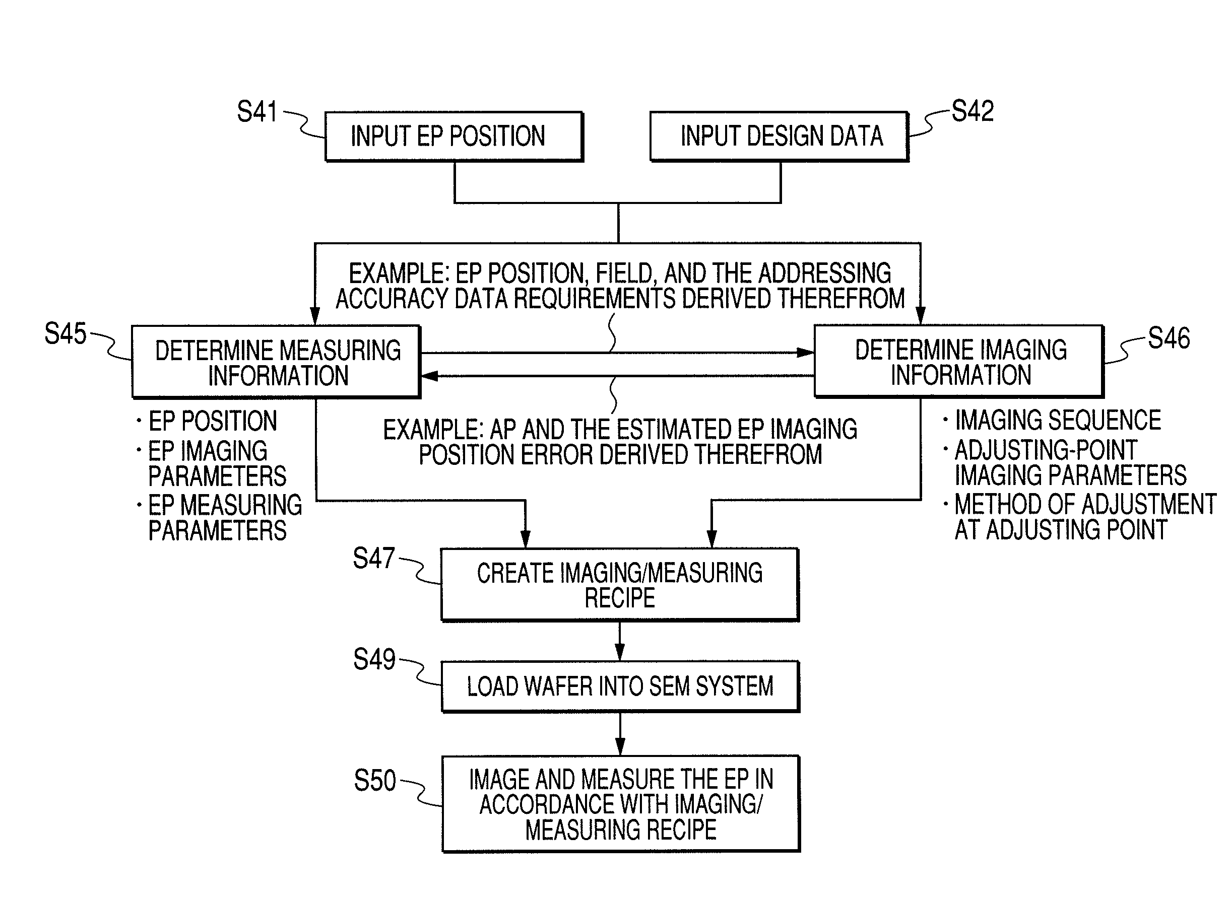
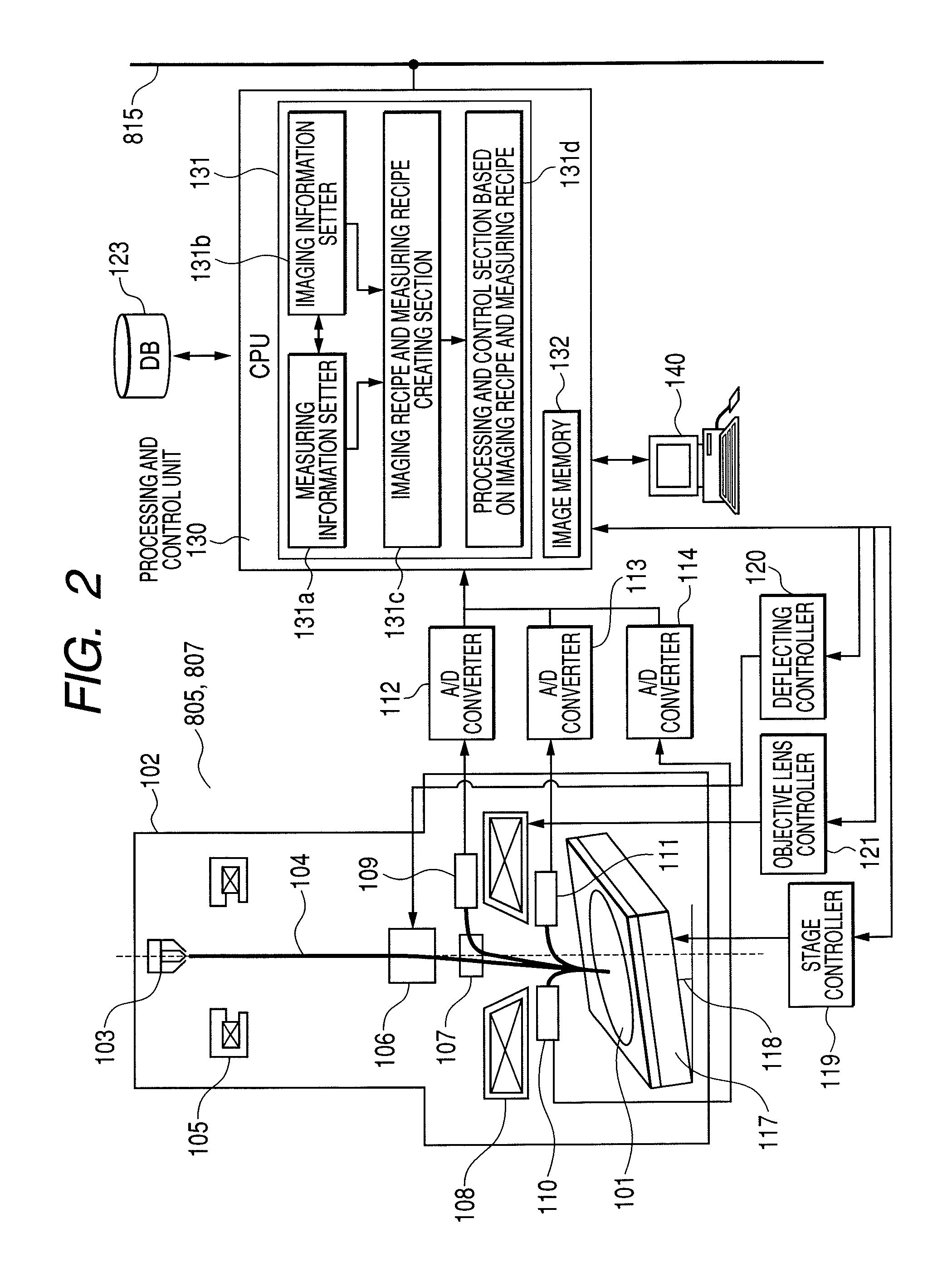
[0049]Embodiments of a SEM (scanning electron microscope) system according to the present invention, the system having an automatic imaging and measuring function to automatically create an imaging recipe or / and measuring recipe in which imaging information or / and measuring information are to be designated, and acquire images using the imaging recipe or / and the measuring recipe, will be described below using FIGS. 1 to 9. Embodiments of a method which uses the above system to execute the above process will also be described.

1. Configuration in which Multiple SEM Systems are Applied to Semiconductor Device Manufacturing Equipment (Database Management and Sharing)

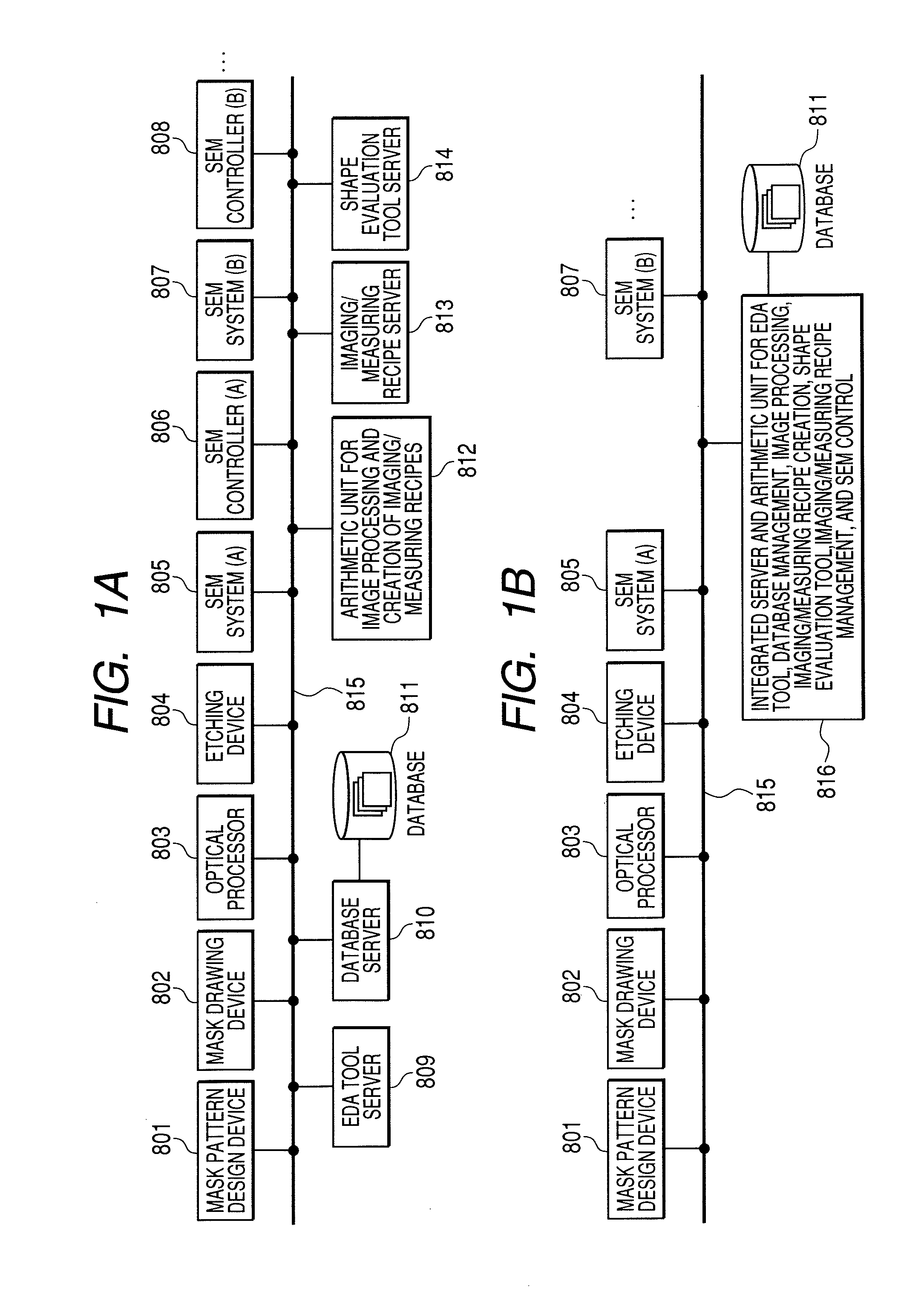
[0050]An embodiment of a configuration in which multiple SEM systems according to the present invention are applied to semiconductor device manufacturing equipment is described below using FIGS. 1A and 1B. Each of the SEM systems has an automatic imaging and measuring function to automatically create an imaging recipe or / and ...


PUM


Abstract

This invention relates to a SEM system constructed to create imaging recipes or / and measuring recipes automatically and at high speed, and improve inspection efficiency and an automation ratio, and to a method using the SEM system; a method for creation of imaging recipes and measuring recipes in the SEM system is adapted to include, in a recipe arithmetic unit, the steps of evaluating a tolerance for an imaging position error level at an evaluation point, evaluating a value predicted of the imaging position error level at the evaluation point when any region on circuit pattern design data is defined as an addressing point, and determining an imaging recipe and a measuring recipe on the basis of a relationship between the tolerance for the imaging position error level at the evaluation point and the predicted value of the imaging position error level at the evaluation point.

Description

BACKGROUND OF THE INVENTION[0001]The present invention relates generally to scanning electron microscope (SEM) systems that can automatically acquire images of any evaluation point on a specimen and evaluate a circuit pattern formed at the evaluation point, and to methods using the SEM systems. More particularly, the invention concerns a SEM system having an imaging recipe and measuring recipe auto-creating function which determines an imaging recipe and measuring recipe constructed to allow acquisition of a SEM image of any evaluation point and desired evaluation for this point (e.g., measurement of line pattern wiring widths or line pattern gaps and extraction of image feature quantities of a defective region). The imaging recipe and measuring recipe is determined from circuit pattern design data automatically and without using an actual wafer. The invention also concerns a method that uses the above SEM system.[0002]A wiring pattern is formed on a semiconductor wafer by applying ...

Claims


Application Information

Patent Timeline
Patent Type & Authority Patents(United States)
IPC IPC(8): G06K9/00
CPCG06T7/0006G06T2207/30148
Inventor MIYAMOTO, ATSUSHINISHIURA, TOMOFUMIMATSUOKA, RYOICHIMOROKUMA, HIDETOSHI
Owner HITACHI HIGH-TECH CORP
Why Eureka
Try Eureka