Bipolar switching of phase change device

a phase change device and bipolar switching technology, applied in semiconductor devices, digital storage, instruments, etc., can solve the problems of difficult to cause an active region of the phase change material, difficult to set,

Active Publication Date: 2011-12-13
MACRONIX INT CO LTD
View PDF380 Cites 25 Cited by
  • Summary
  • Abstract
  • Description
  • Claims
  • Application Information

AI Technical Summary

Benefits of technology

The operations described herein comprising set and reset bias arrangements having opposite polarity pulses have been demonstrated to overcome the “difficult to set” behavior of memory cell structures such as small bridge-type memory cells which suffer significant thermoelectric effects that cause asymmetrical heating in the body of the phase change material. Representative configurations suffering this “difficult to set” behavior have an active region with a heating zone during a set operation which is spaced away from electrodes contacting the phase change material.
In embodiments the second voltage pulse of the set bias arrangement has a pulse width of 60 ns or less. As a result, the phase change memory devices and methods for operating described herein overcome the slow set behavior commonly associated with phase change memory devices, and extend their usefulness into high speed applications such as DRAM which require a set pulse width less than or equal to 60 ns.

Problems solved by technology

However, reducing the size of the phase change memory element can result in a “difficult to set” phenomenon.
Specifically, it can be become difficult to cause an active region of the phase change material to transition from the amorphous phase of the high resistance state 102 to the crystalline phase of the lower resistance state 100.

Method used


Image

  • Bipolar switching of phase change device
  • Bipolar switching of phase change device
  • Bipolar switching of phase change device

Examples


Embodiment Construction

The following description of the disclosure will typically be with reference to specific structural embodiments and methods. It is to be understood that there is no intention to limit the disclosure to the specifically disclosed embodiments and methods, but that the disclosure may be practiced using other features, elements, methods and embodiments. Preferred embodiments are described to illustrate the present disclosure, not to limit its scope, which is defined by the claims. Those of ordinary skill in the art will recognize a variety of equivalent variations on the description that follows. Like elements in various embodiments are commonly referred to with like reference numerals.

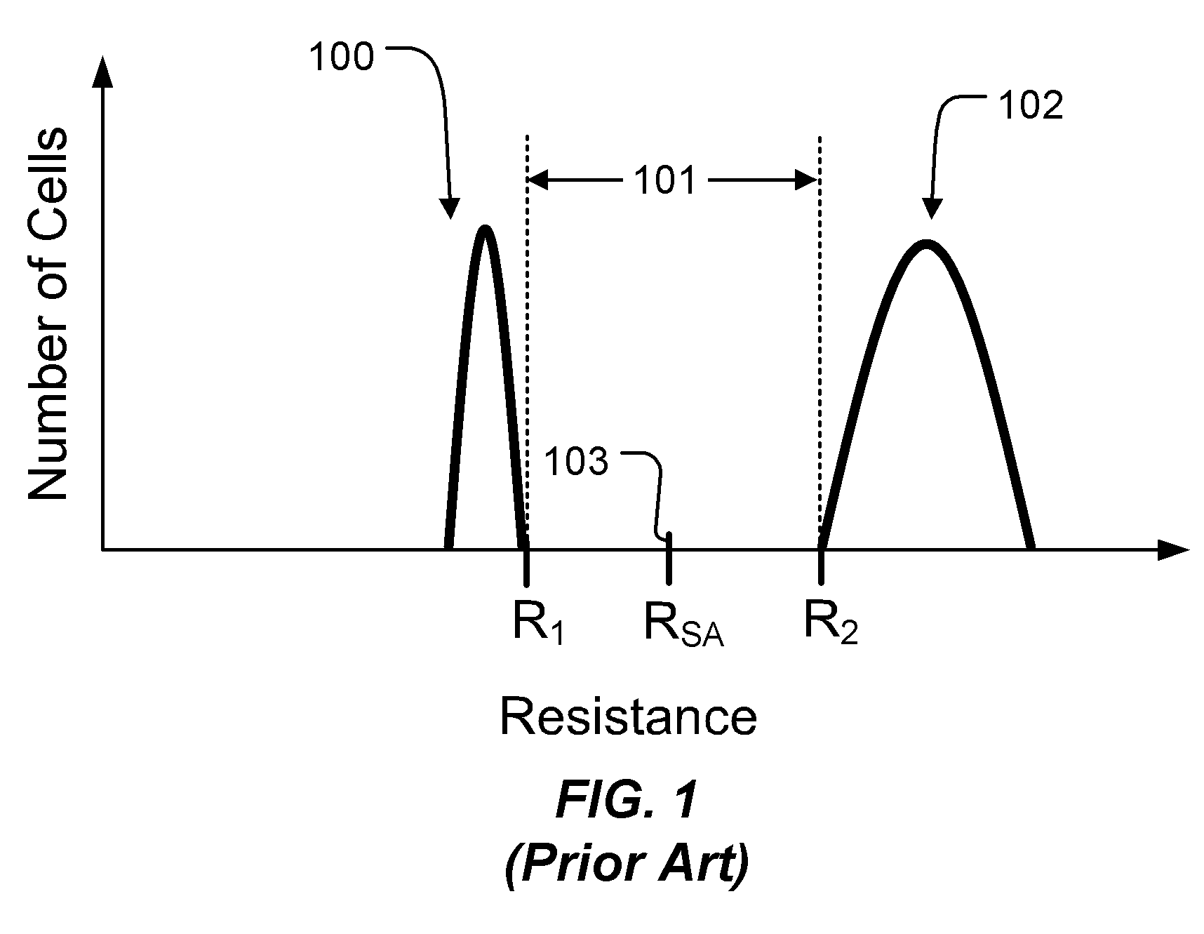
As mentioned above, as the size of the phase change memory element is reduced it can become more and more difficult to cause a transition to the lower resistance state 100.

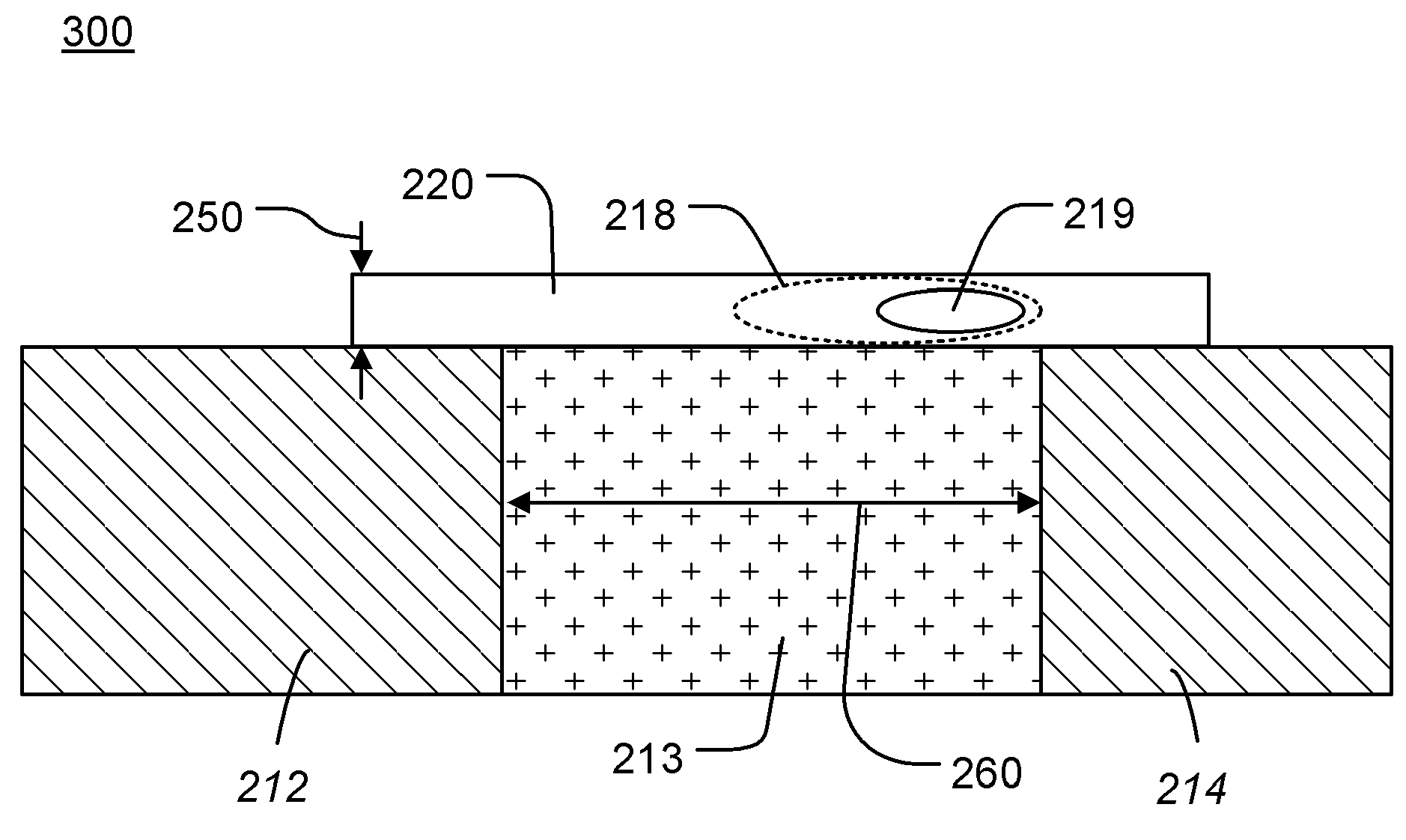
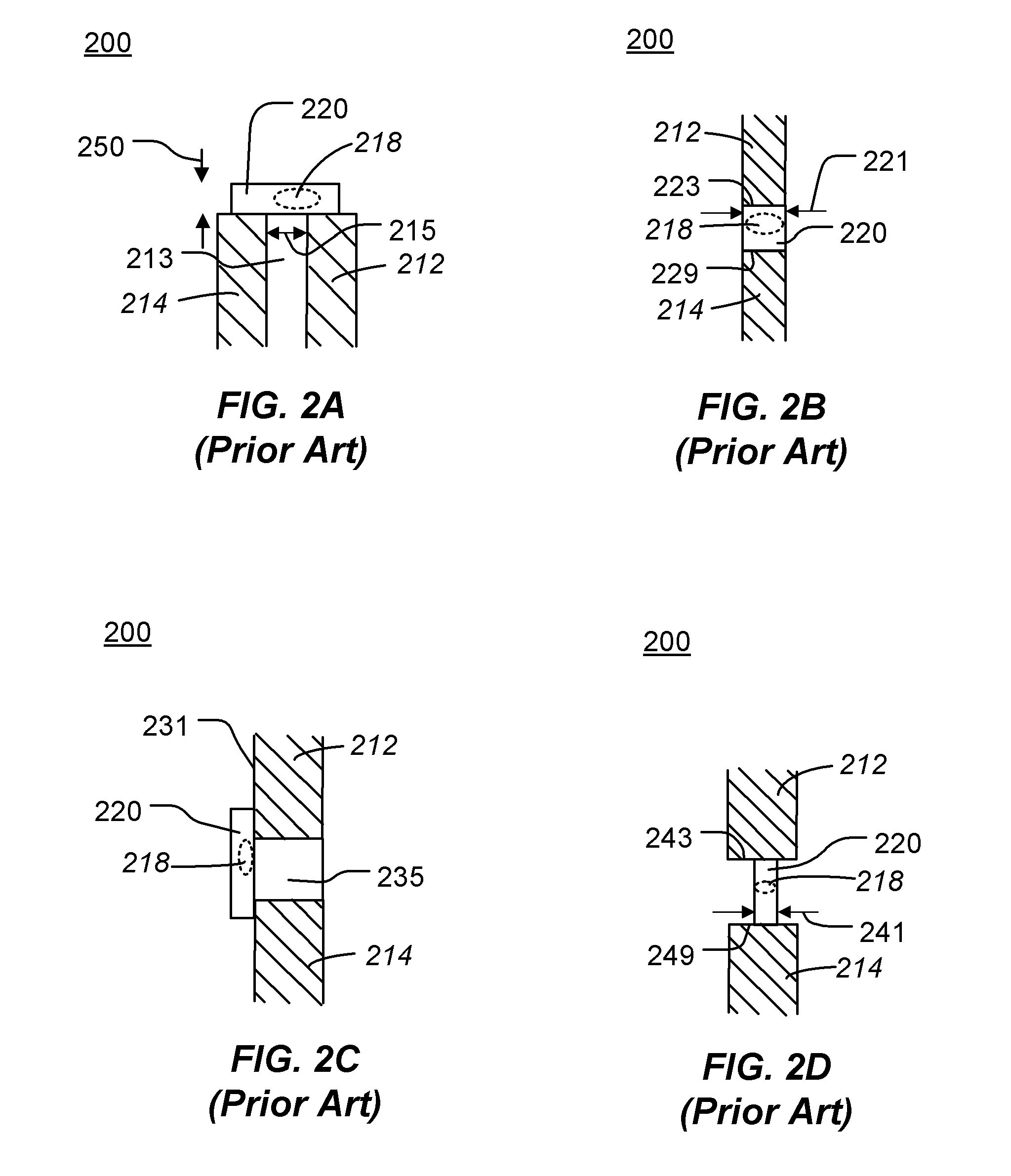
FIGS. 2A-2D show representative prior art memory cell structures for which the bipolar operations described herein can be applied to o...


PUM


Abstract

Memory devices and methods for operating such devices are described herein. A method as described herein includes applying a reset bias arrangement to a memory cell to change the resistance state from the lower resistance state to the higher resistance state. The reset bias arrangement comprises a first voltage pulse. The method further includes applying a set bias arrangement to the memory cell to change the resistance state from the higher resistance state to the lower resistance state. The set bias arrangement comprises a second voltage pulse, the second voltage pulse having a voltage polarity different from that of the first voltage pulse.

Description

BACKGROUND OF THE INVENTION1. Field of the InventionThe present invention relates to memory devices based on phase change based memory materials, including chalcogenide based materials and on other programmable resistive materials, and methods for operating such devices.2. Description of Related ArtPhase change based memory materials, like chalcogenide based materials and similar materials, can be caused to change phase between an amorphous state and a crystalline state by application of electrical current at levels suitable for implementation in integrated circuits. The generally amorphous state is characterized by higher electrical resistivity than the generally crystalline state, which can be readily sensed to indicate data. These properties have generated interest in using programmable resistive material to form nonvolatile memory circuits, which can be read and written with random access.In phase change memory, data is stored by causing transitions in an active region of the ph...

Claims


Application Information

Patent Timeline
Patent Type & Authority Patents(United States)
IPC IPC(8): G11C11/00
CPCG11C11/5678G11C13/0004G11C13/0064G11C13/0069G11C2013/0092G11C2013/0073G11C2013/0078
Inventor CHEN, YI-CHOULIN, YUYU
Owner MACRONIX INT CO LTD
Why Eureka
Try Eureka