Integrated MEMS metrology device using complementary measuring combs

a technology of complementary measuring combs and metrology devices, which is applied in the direction of acceleration measurement using interia forces, using mechanical means, instruments, etc., can solve the problems of inability to have an equivalent in-situ device in the mems world, inability to achieve in-situ measurement capability of mems devices, and inability to meet the needs of measurement and monitoring, etc., to achieve accurate measurement and monitoring, and compact size

Inactive Publication Date: 2011-12-20
RGT UNIV OF CALIFORNIA
View PDF3 Cites 8 Cited by
  • Summary
  • Abstract
  • Description
  • Claims
  • Application Information

AI Technical Summary

Benefits of technology

[0010]The embodiments of the present invention enable the in-situ monitoring of material, process and dynamic properties of MEMS devices. The MEMS metrology devices of the present invention enable a nondestructive metrology scheme, are inexpensive and thus are deployable in arrays. They are also compact in size and so are ideal for on-chip integration and thus can be constructed in close proximity to the MEMS devices being monitored. In addition, the MEMS metrology devices in accordance with the embodiments of the present invention provide for accurate measurements and monitoring of material, process and dynamic properties of MEMS devices.

Problems solved by technology

It has been determined that the performance of such devices changes in time due in part to changes in their material properties, which result in part from changes in thermal and load or shock cycles.
So, while in the CMOS world E-test devices are available that can be incorporated in the masks used to manufacture the CMOS devices, no such equivalent in-situ device exists in the MEMS world.
This lack of in-situ measurement capability for MEMS devices is further complicated due to the fact that MEMS devices are movable and that an aspect of their related measurement is directed to measuring the mechanical properties of the MEMS devices.
These approaches tend to be very expensive to implement requiring the use of expensive equipment and highly qualified operators.
Such a test is sensitive to process variations and cannot measure geometric properties, such as the line width of the device.
This test is however restricted to the measurement of out-of-plane characteristics of a beam.

Method used


Image

  • Integrated MEMS metrology device using complementary measuring combs
  • Integrated MEMS metrology device using complementary measuring combs
  • Integrated MEMS metrology device using complementary measuring combs

Examples


Embodiment Construction

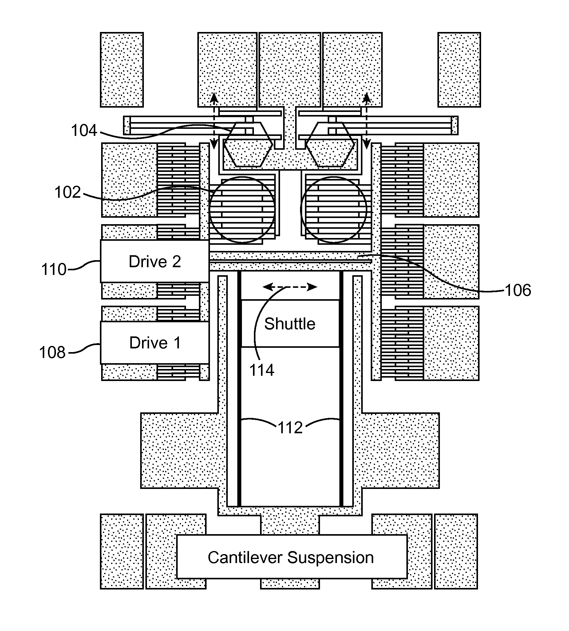
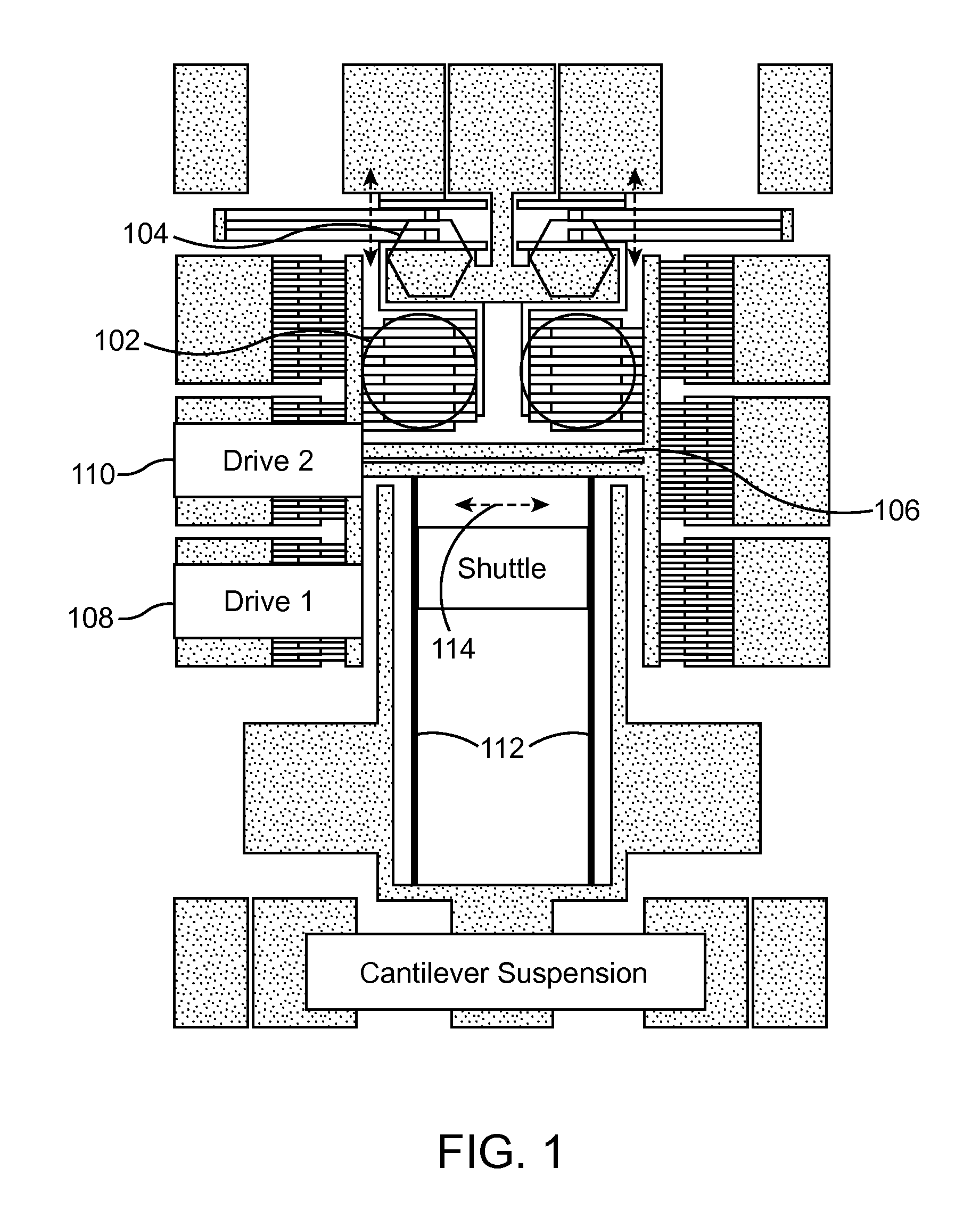
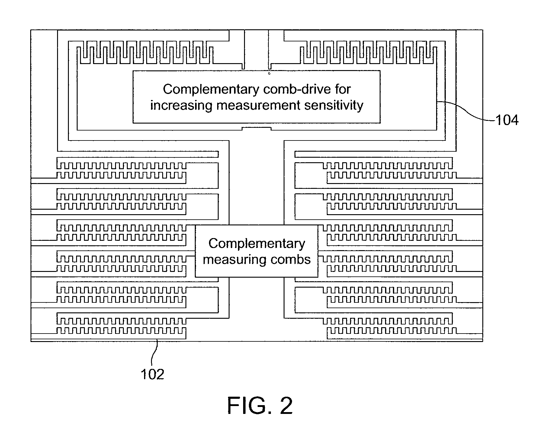
[0023]FIG. 1 shows a device layout of a MEMS metrology device in accordance with an embodiment of the present invention. FIG. 2 is a detail view of the complementary measuring combs 102 of the device of FIG. 1. FIG. 2 also shows the complementary comb-drive 104 that is used for increasing measurement sensitivity. In the device of FIG. 1, capacitance changes across the measuring combs 102 correspond with the lateral translation of the shuttle 106 as it is actuated by the comb-drives (e.g., drives 108 and 110). The device of FIG. 1 can be a compact device, fitting inside a 1 mm by 1 mm square or smaller, that can accurately measure in-plane over- or under-cut, effective Young's Modulus, and the comb-drive force for the material and process in which it is made. This device is useful for nanoscale calipers, manipulators, and force gauges, as well as for the scientific exploration of physical forces, developing fabrication processes, calibrating simulations of devices, and automatically ...


PUM


Abstract

The present invention provides a device for in-situ monitoring of material, process and dynamic properties of a MEMS device. The monitoring device includes a pair of comb drives, a cantilever suspension comprising a translating shuttle operatively connected with the pair of comb drives, structures for applying an electrical potential to the comb drives to displace the shuttle, structures for measuring an electrical potential from the pair of comb drives; measuring combs configured to measure the displacement of the shuttle, and structures for measuring an electrical capacitance of the measuring combs. Each of the comb drives may have differently sized comb finger gaps and a different number of comb finger gaps. The shuttle may be formed on two cantilevers perpendicularly disposed with the shuttle, whereby the cantilevers act as springs to return the shuttle to its initial position after each displacement.

Description

CROSS REFERENCE TO RELATED APPLICATIONS[0001]This application claims the benefit of priority from U.S. provisional patent application No. 60 / 793,424, filed Apr. 19, 2006, the entirety of which is incorporated herein by reference.STATEMENT AS TO RIGHTS TO INVENTIONS MADE UNDER FEDERALLY SPONSORED RESEARCH AND DEVELOPMENT[0002]This invention was made with Government support under NSF Grant Nos. EIA-0122599 and EEC-0318642. The Government has certain rights to this invention.BACKGROUND OF THE INVENTION[0003]The present invention relates to a Micro-Electromechanical System (MEMS) metrology device and techniques for using the device to measure geometric, dynamic, and material properties of MEMS devices.[0004]MEMS devices are known. MEMS devices typically include a two-and-one-half dimension (2.5D) structure that has movable and anchored portions. A common MEMS device having such a structure is a MEMS accelerometer such as the NASA Electronic Part and Package (NEEP) 2001. Such a device in...

Claims


Application Information

Patent Timeline
Patent Type & Authority Patents(United States)
IPC IPC(8): G01P21/00B81C99/00
CPCB81C99/005H02N1/008G02B26/0841
Inventor GARMIRE, DAVIDCHOO, HYUCKMULLER, RICHARD S.DEMMEL, JAMESGOVINDJEE, SANJAY
Owner RGT UNIV OF CALIFORNIA
Why Eureka
Try Eureka