
Semiconductor devices and electrical parts manufacturing using metal coated wires

a technology of metal coated wires and semiconductor devices, applied in semiconductor devices, semiconductor/solid-state device details, electrical apparatus, etc., can solve problems such as inability to reliably connect copper, wire or bond breakage, etc., to reduce manufacturing costs, eliminate plating bare copper lead frames, and no loss of reliability

Inactive Publication Date: 2011-12-27
SEMICON COMPONENTS IND LLC
View PDF6 Cites 2 Cited by
  • Summary
  • Abstract
  • Description
  • Claims
  • Application Information

AI Technical Summary

Benefits of technology

The present invention provides a semiconductor device with bond pads for receiving a bond wire, and a method of manufacturing the device using a coated wire. The wire is coated with metal to eliminate the need for plating of the lead frame, reducing manufacturing costs. The coated wire eliminates potential failures of other metallurgic systems and ensures reliability of the system. The technical effects of the invention include reducing manufacturing costs and ensuring reliability of the semiconductor device.

Problems solved by technology

However, Aluminum and copper, for instance, are not known to have a reliable connection.
Aluminum and copper create several intermetallic phases that are brittle and that lower shear strength at certain temperatures which increase the growth of brittle copper-aluminum intermetallic phases, and thereby cause breakage in the wire or bond.

Method used


Image

  • Semiconductor devices and electrical parts manufacturing using metal coated wires
  • Semiconductor devices and electrical parts manufacturing using metal coated wires
  • Semiconductor devices and electrical parts manufacturing using metal coated wires

Examples


Embodiment Construction

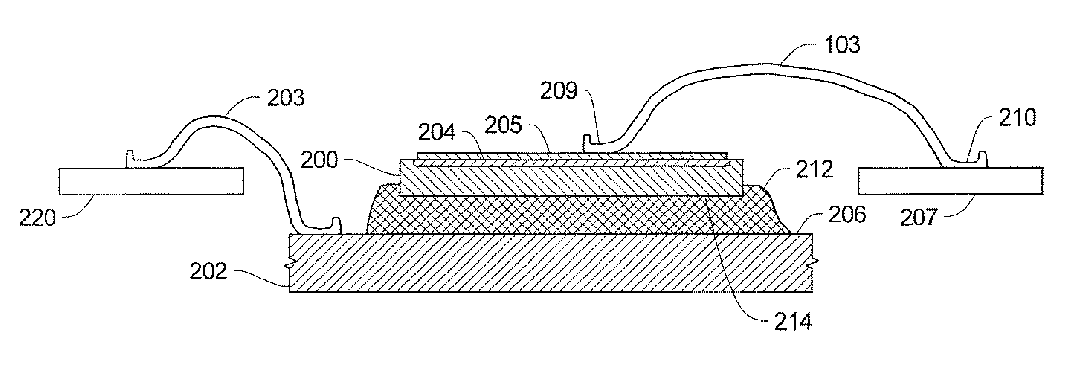
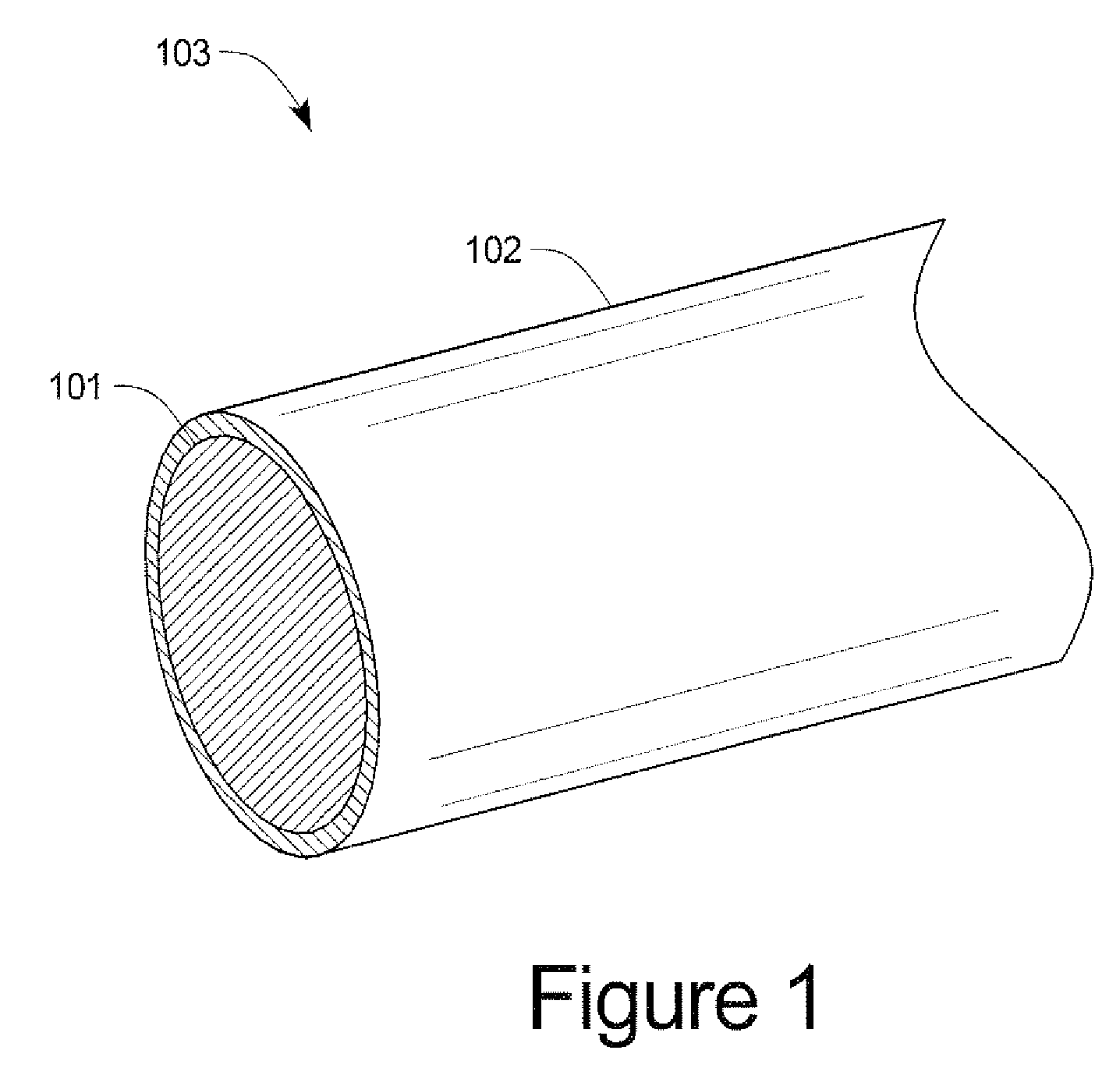
[0014]FIG. 1 shows a coated aluminum wire 103. An aluminum wire 101 is coated with a metallic material 102, and is used for creating an electrical connection between a semiconductor die and leads during packaging of the device and is more generally used for connecting electrical parts. The wire 101 may be pure aluminum, but may also be an aluminum alloy with silicon or magnesium as a strengthening mechanism. The coating 102 may be a copper compatible metal such as nickel or palladium.

[0015]The coating 102 is plated onto the aluminum wire 101 either by electroless or electrical plating. For both processes, the aluminum wire is first prepared for plating by cleaning the surface of the wire to improve adhesion of the metal coating to the surface of the aluminum wire 101. This can be accomplished by methods known in the art, such as using detergents or solvents to remove grease, environmental contaminants, oxides and other undesirable materials that can affect the ability of the metal c...


PUM

PropertyMeasurementUnit
metallicaaaaaaaaaa
shear strengthaaaaaaaaaa
temperaturesaaaaaaaaaa

Abstract

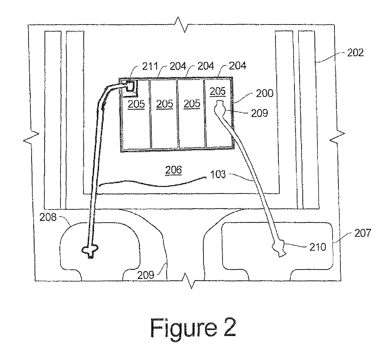
The device of this invention includes a semiconductor die attached to a bare copper lead frame and electrically coupled to a lead by a metal wire coated with a metallic material. The device would function similarly to devices where the lead frames were coated with other metallic materials, but at lower costs because instead of plating the lead frame the wire is plated. The wire can be either gold or aluminum. When the wire is gold, the coating may be silver or other suitable metallic materials. When the wire is aluminum, the coating may be nickel, palladium, or other suitable metals.

Description

CROSS-REFERENCE TO RELATED APPLICATIONS[0001]This application claims the benefit of U.S. Provisional Patent Application Ser. No. 60 / 786,259, filed Mar. 27, 2006 which is hereby incorporated by reference.FIELD OF THE INVENTION[0002]This invention relates to a packaged semiconductor device, and more specifically, to a semiconductor device having a metal wire coated with a metallic material used for wire bonding and to the use of coated wires for the connection of electronic parts.BACKGROUND OF THE INVENTION[0003]Generally a packaged semiconductor device includes a semiconductor die attached to a copper lead frame plated with other metals, such as nickel or silver. The die is then connected to leads by bonding wires made from, generally, aluminum, gold, or copper to a wire bond site on the die and bonded on its second end to a corresponding lead. For example, an aluminum wire on its first end is bonded to a source contact on the die and its second end is bonded to a source lead. Therea...

Claims


Application Information

Patent Timeline
Patent Type & Authority Patents(United States)
IPC IPC(8): H01L23/48
CPCH01L24/45H01L24/49H01L24/32H01L24/83H01L24/85H01L2224/32245H01L2224/45124H01L2224/45144H01L2224/45565H01L2224/456H01L2224/45639H01L2224/45655H01L2224/45664H01L2224/48091H01L2224/48247H01L2224/48472H01L2224/49H01L2224/73265H01L2224/83801H01L2224/85205H01L2924/01002H01L2924/01004H01L2924/01005H01L2924/01006H01L2924/01012H01L2924/01013H01L2924/01014H01L2924/01015H01L2924/01028H01L2924/01029H01L2924/01033H01L2924/01046H01L2924/01047H01L2924/01078H01L2924/01079H01L2924/01082H01L2924/01327H01L2924/13055H01L2924/13091H01L2924/14H01L2924/19043H01L2924/19107H01L2924/20104H01L2924/20105H01L2924/20107H01L2924/014H01L2924/0132H01L24/29H01L2224/85447H01L2924/15747H01L2224/29101H01L2924/1306H01L2924/1301H01L2924/13034H01L2924/1305H01L2924/00014H01L2924/00011H01L2924/00H01L2924/00012H01L2924/013H01L2224/45147H01L2224/48847H01L2224/48647H01L2224/48747H01L24/48H01L2224/85207H01L2924/00015H01L2924/00013H01L2224/83205H01L2224/43848
Inventor LEE, SANGDOKWON, YONKSUKCAI, BIN
Owner SEMICON COMPONENTS IND LLC
Learn More