Manufacturing method of package-on-package structure

a manufacturing method and packaging technology, applied in the direction of electrical equipment, semiconductor devices, semiconductor/solid-state device details, etc., can solve the problems of thin pop structure with lower manufacturing cost, and achieve the effect of reducing the overall thickness of the package structure, reducing the thickness of the encapsulant, and improving heat dissipation efficiency

Inactive Publication Date: 2019-01-01
POWERTECH TECHNOLOGY INC
View PDF7 Cites 0 Cited by
  • Summary
  • Abstract
  • Description
  • Claims
  • Application Information

AI Technical Summary

Benefits of technology

[0004]The disclosure provides a manufacturing method of a package-on-package (POP) structure, which reduces the overall thickness and the manufacturing cost thereof.
[0007]Based on the above, since the thickness of the encapsulant is reduced and also the plate of the conductive interposer is removed to form the first package structure, the conductive pillars of the conductive interposer exposed from the encapsulant may serve as the electrical connecting path between the first package structure and the second package structure and the conductive protrusion may exposed from the encapsulant may serve as the heat sink for a better heat dissipation efficiency. In other word, it is unnecessary to dispose additional interposer between the first package structure and the second package structure for electrical connection therebetween. The overall thickness reduction in the package structure can be reduced after removing a portion of the encapsulant and a plate of the conductive interposer, thereby achieving package miniaturization. The thermal interface material formed on the top surface of the conductive protrusion is conducive to bond the second package structure to the first package structure and improve the heat dissipation from the first package structure. When providing the conductive interposer on the circuit carrier, the alignment window may be aligned with the die. That is, it is no need to form additional alignment mark to align the conductive interposer with the die. Hence, the overall thickness of the POP structure may be reduced and the lower manufacturing costs may be achieved.

Problems solved by technology

As such, how to achieve a thinner POP structure with lower manufacturing cost has become a challenge to researchers in the field.

Method used


Image

  • Manufacturing method of package-on-package structure
  • Manufacturing method of package-on-package structure
  • Manufacturing method of package-on-package structure

Examples


Embodiment Construction

[0013]Reference will now be made in detail to the present preferred embodiments of the disclosure, examples of which are illustrated in the accompanying drawings.

[0014]Wherever possible, the same reference numbers are used in the drawings and the description to refer to the same or like parts.

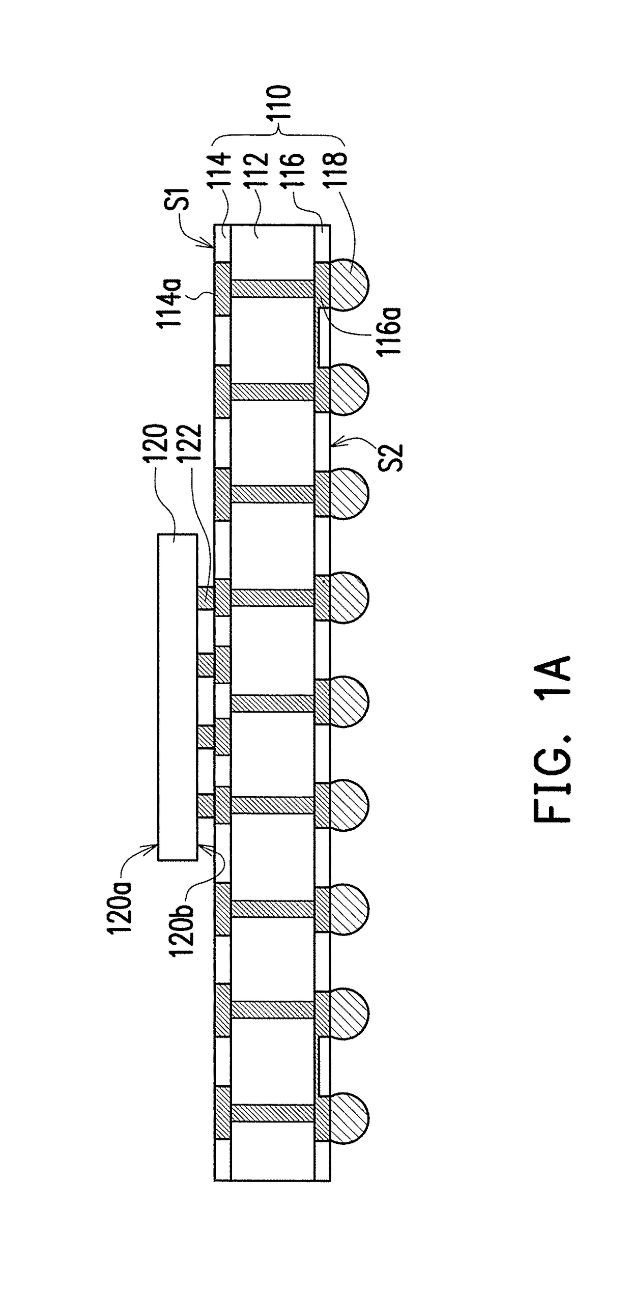
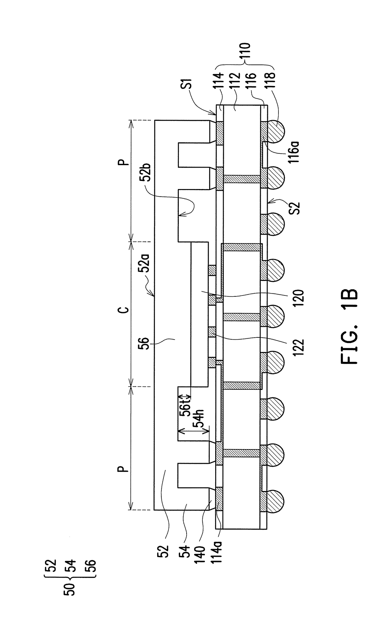
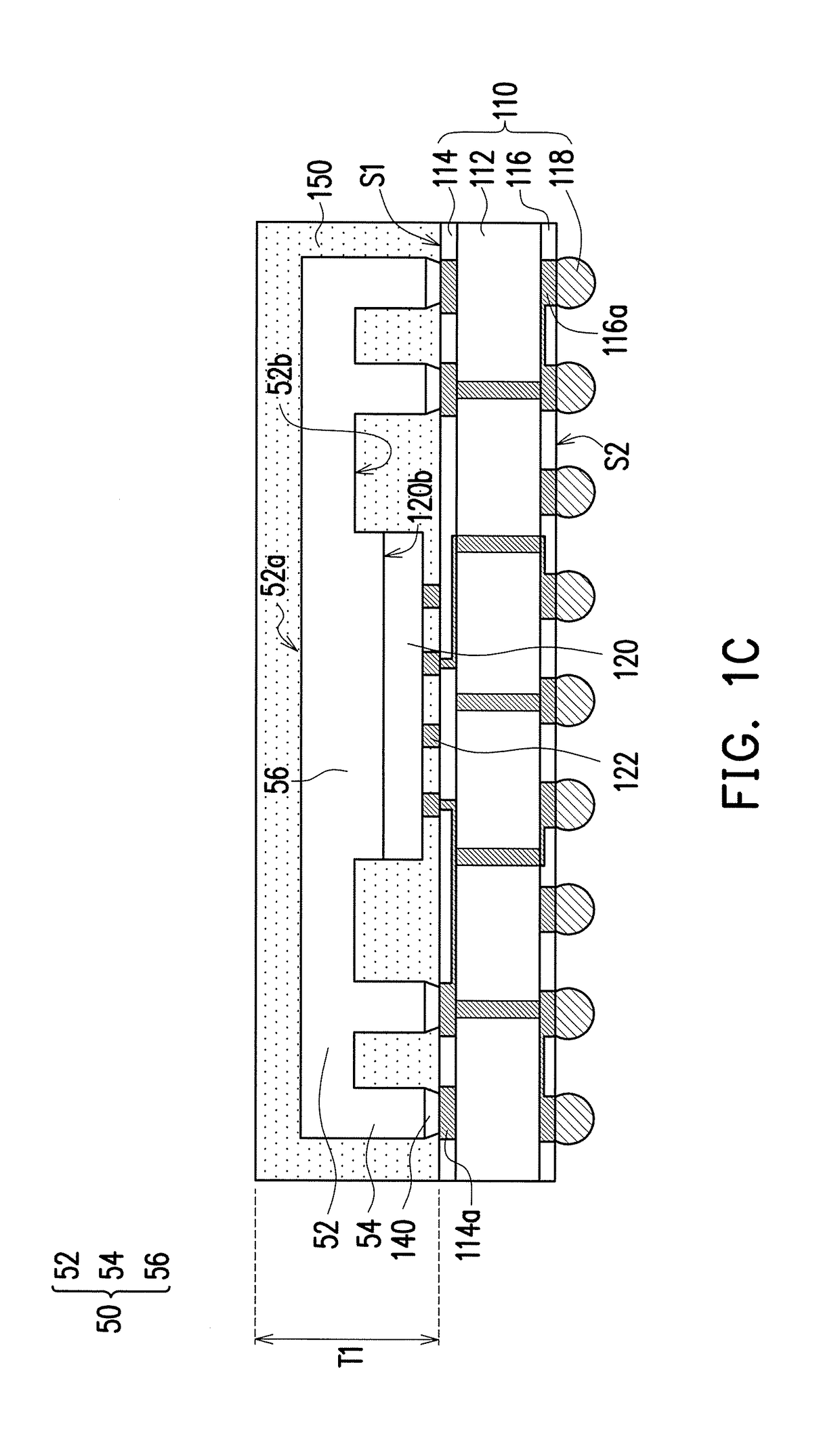
[0015]FIG. 1A to FIG. 1E are schematic cross-sectional views illustrating manufacturing method of a POP structure according to an embodiment of the disclosure. Referring to FIG. 1A, a first circuit carrier 110 is provided and a first die 120 is bonded on the first circuit carrier 110. The first circuit carrier 110 may have a top surface S1 and a bottom surface S2 opposite to the top surface S1. For example, the first circuit carrier 110 may include a core layer 112, a top circuit layer 114 disposed on the top surface S1 and the bottom circuit layer 116 disposed on the bottom surface S2 of the first circuit carrier 110. The core layer 112 is disposed between and electrically connects the top cir...


PUM


Abstract

A manufacturing method of a POP structure including at least the following steps is provided. A first package structure is formed and a second package structure is formed on the first package structure. The first package structure includes a circuit carrier and a die disposed on the circuit carrier. Forming the first package structure includes providing a conductive interposer on the circuit carrier, encapsulating the conductive interposer by an encapsulant and removing a portion of the encapsulant and the plate of the conductive interposer. The conductive interposer includes a plate, a plurality of conductive pillars and a conductive protrusion respectively extending from the plate to the circuit carrier and the die. The conductive protrusion disposed on the die, and the conductive pillars are electrically connected to the circuit carrier. The second package structure is electrically connected to the first package structure through the conductive interposer.

Description

CROSS REFERENCE TO RELATED APPLICATION[0001]This application claims the priority benefit of U.S. provisional application Ser. No. 62 / 410,851, filed on Oct. 21, 2016. The entirety of the above-mentioned patent application is hereby incorporated by reference herein and made a part of the specification.BACKGROUND OF THE INVENTION1. Field of the Invention[0002]The present invention generally relates to a manufacturing method of a package structure, and more particularly relates to a manufacturing method of a package-on-package (POP) structure.2. Description of Related Art[0003]In order for electronic product design to achieve being light, slim, short, and small, semiconductor packaging technology has kept progressing, in attempt to develop products that are smaller in volume, lighter in weight, higher in integration, and more competitive in the market. For example, 3D stacking technologies such as POP have been developed to meet the requirements of higher packaging densities. As such, h...

Claims


Application Information

Patent Timeline
Patent Type & Authority Patents(United States)
IPC IPC(8): H01L23/00H01L25/00H01L21/48H01L23/31H01L23/498H01L25/10H01L23/49H01L23/50H01L21/56H01L23/538H01L25/065H01L23/04H01L23/433
CPCH01L25/50H01L21/486H01L21/4853H01L21/4889H01L21/56H01L21/563H01L21/565H01L23/04H01L23/3121H01L23/3128H01L23/4334H01L23/49H01L23/49811H01L23/49816H01L23/49827H01L23/49833H01L23/50H01L23/5384H01L24/03H01L24/11H01L24/27H01L24/83H01L24/97H01L25/0657H01L25/105H01L23/49838H01L24/13H01L24/16H01L24/29H01L24/32H01L24/45H01L24/48H01L24/73H01L24/92H01L2224/03H01L2224/0401H01L2224/04042H01L2224/13023H01L2224/13147H01L2224/16227H01L2224/16235H01L2224/16237H01L2224/2919H01L2224/29139H01L2224/32225H01L2224/32245H01L2224/45144H01L2224/45147H01L2224/48091H01L2224/48227H01L2224/48235H01L2224/73253H01L2224/73265H01L2224/92225H01L2225/1023H01L2225/1035H01L2225/1041H01L2225/1058H01L2225/1088H01L2225/1094H01L2924/1431H01L2924/1433H01L2924/1533H01L2924/15311H01L2924/181H01L21/50H01L24/82H01L24/81H01L24/85H01L23/3107H01L23/3672H01L25/18H01L21/561H01L25/071H01L2224/3224H01L2224/85007H01L2224/82047H01L2224/81H01L2224/83007H01L23/42H01L2224/08245H01L2224/73251H01L2224/85181H01L2224/85186H01L2224/83101H01L2224/29339H01L2224/29294H01L24/08H01L2224/92222H01L24/80H01L2924/00012H01L2924/00014H01L2224/08H01L2224/16H01L2224/80H01L2924/00
Inventor WANG, CHI-ANHSU, HUNG-HSIN
Owner POWERTECH TECHNOLOGY INC
Why Eureka
Try Eureka