
System and method for RF shielding of a semiconductor package

a technology of shielding and semiconductors, applied in semiconductor devices, semiconductor/solid-state device details, electrical equipment, etc., can solve problems such as the inability to solve the problem of multi-tier wire fences, the shield effectiveness of mold cavities, and the reduction of existing solutions such as wire fences and via ablation

Active Publication Date: 2012-01-10
AMKOR TECH SINGAPORE HLDG PTE LTD
View PDF26 Cites 91 Cited by
  • Summary
  • Abstract
  • Description
  • Claims
  • Application Information

AI Technical Summary

Problems solved by technology

Presently, there are issues with shield effectiveness in mold cavities.
Existing solutions such as wire fence and via ablation have reduced performance as the mold cap gets thicker because the gap between ground structures increases.
Even multi-tier wire fence cannot resolve this issue completely.
In this type of packaging, a wire fence may be required to shield the perimeter of the module because it may be difficult to perform laser ablation of the TMV vias after singulating the units as is required for a full saw shield structure.
Wire fence may be difficult to implement on a two tier structure.

Method used


Image

  • System and method for RF shielding of a semiconductor package
  • System and method for RF shielding of a semiconductor package
  • System and method for RF shielding of a semiconductor package

Examples


Embodiment Construction

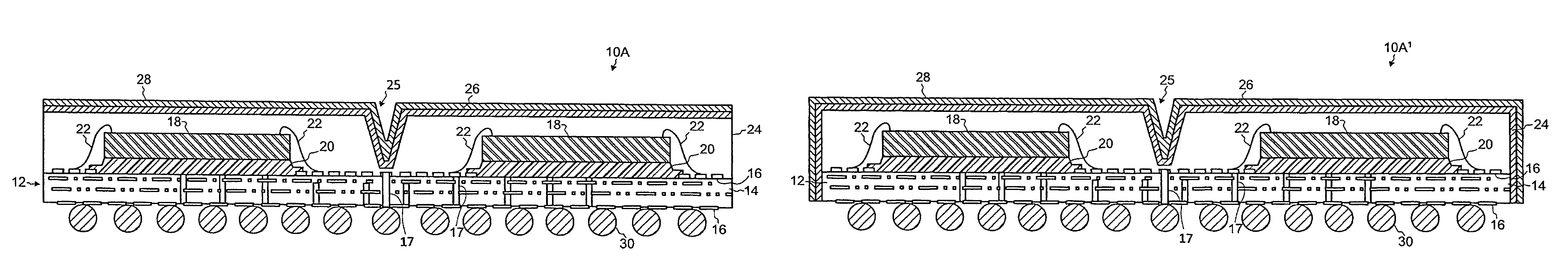
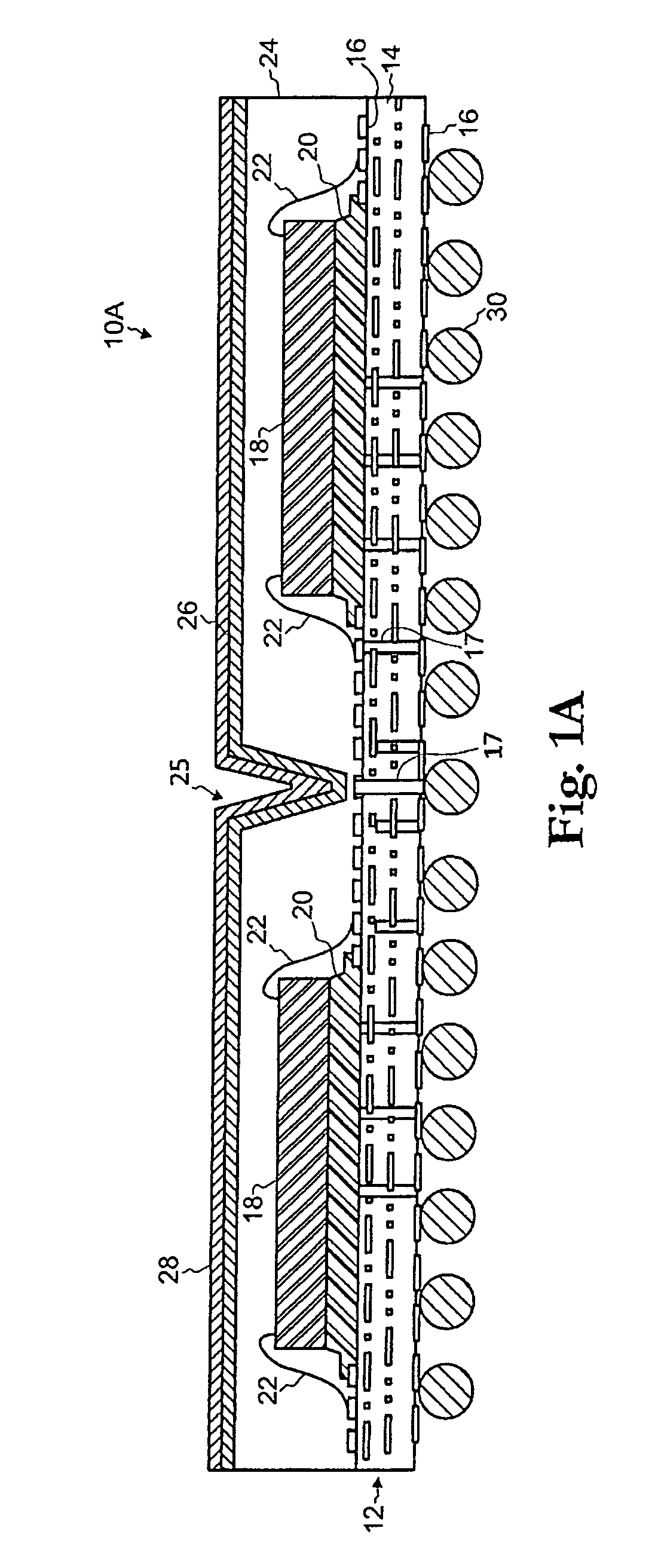
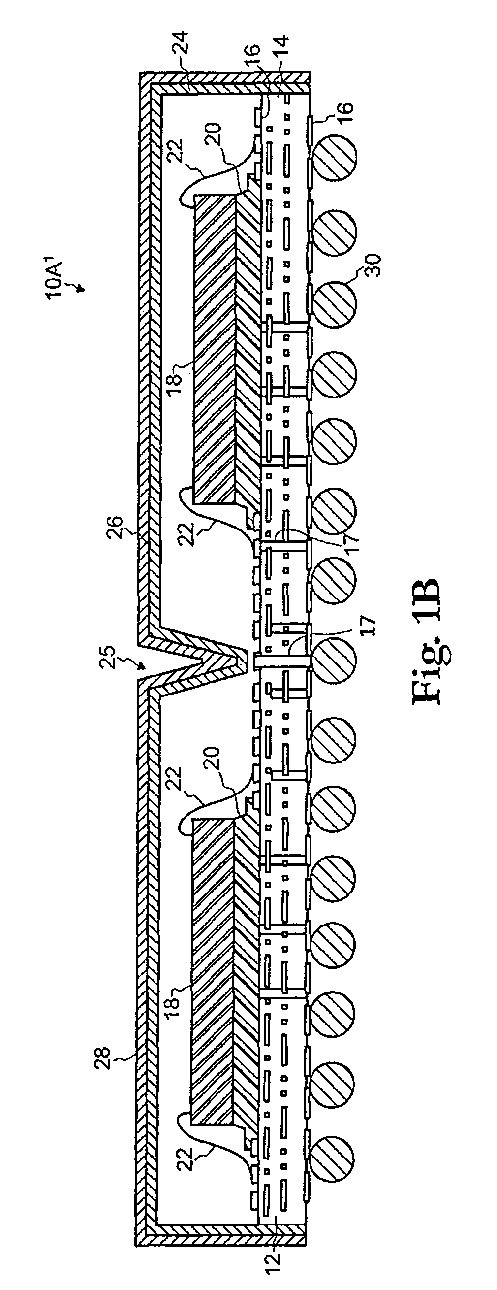
[0040]Referring to FIG. 1A, a semiconductor device 10A (hereinafter device 10A) is shown. The device 10A has a substrate 12. The substrate 12 may be any one chosen from a conventional rigid PCB, a flexible PCB, and an equivalent thereof, but the kind of substrate 12 is not limited herein. The substrate 12 may include an insulation layer 14 having predetermined area and thickness. The insulation layer 14 may have an approximately planar first surface and an approximately planar second surface opposing the first surface. The substrate 12 may have a plurality of metal traces 16 formed on the first surface of the insulation layer 14. A plurality of metal traces 16 may also be formed on the second surface of the insulation layer 14. The number of metal traces 16 is not limited to the number shown in the FIG. 1A. If multiple layers of metal traces 16 are formed, a dielectric layer may be applied between the metal traces 16. The dielectric layer may be used as an insulating layer to separa...


PUM


Abstract

A semiconductor device has a substrate having a plurality of metal traces. At least one electronic component is electrically coupled to a first surface of the substrate. A mold compound is used for encapsulating portions of the electronic component and the first surface of the substrate, wherein a portion of the mold compound is removed around at least one side of the electronic component. A conductive coating is applied to the mold compound and an area where the portion of the mold compound is removed.

Description

FIELD OF THE INVENTION[0001]This invention relates to Radio Frequency (RF) shielding and, more specifically, to a system and method for providing full package and compartmental shielding in a semiconductor package that provides a more effective shielding method than conformal shielding alone.BACKGROUND OF THE INVENTION[0002]Radio Frequency (RF) shielding may be required on certain semiconductor devices and modules (hereinafter semiconductor device) in order to minimize Electro-Magnetic Interference (EMI) radiation from the semiconductor device. RF shielding is further required to prevent RF radiation from external sources from interfering with operation of the semiconductor device. In a semiconductor device which integrates multiple functions / modules (front end module+transmitter, radio+baseband, etc.) compartmental shielding may be required to minimize EMI radiation from the different components / modules and to prevent RF radiation from interfering with operation of the different co...

Claims


Application Information

Patent Timeline
IPC IPC(8): H01L23/552H01L23/48H01L29/40H01L23/52H01L23/28
CPCH01L23/3128H01L25/0655H01L24/97H01L23/552H01L23/49805H01L2924/3025H01L2924/19107H01L2924/014H01L2924/01075H01L2924/01033H01L2924/1815H01L2924/1617H01L2924/15311H01L2924/078H01L2924/01078H01L2224/97H01L2224/73265H01L2224/48227H01L2224/48091H01L2224/32225H01L24/48H01L24/32H01L24/29H01L24/16H01L2224/85H01L2224/83H01L2924/00014H01L2924/00012H01L2924/00H01L2924/181H01L24/73H01L2224/45099H01L2224/45015H01L2924/207
Inventor FUENTES, RUBENSCANLAN, CHRISTOPHERCHUN, JONG
Owner AMKOR TECH SINGAPORE HLDG PTE LTD
Features
  • Generate Ideas
  • Intellectual Property
  • Life Sciences
  • Materials
  • Tech Scout
  • Unparalleled Data Quality
  • Higher Quality Content
  • 60% Fewer Hallucinations
Learn More