AD converter

a converter and analog-to-digital technology, applied in the field of analog-to-digital converters, can solve problems such as the difficulty of applying the ad converter b>, and achieve the effects of reducing power consumption, reducing area, and minimizing overrange exten

Inactive Publication Date: 2012-01-31
SONY CORP
View PDF8 Cites 112 Cited by
  • Summary
  • Abstract
  • Description
  • Claims
  • Application Information

AI Technical Summary

Benefits of technology

[0010]Therefore, it is desirable to provide an AD converter of reduced power consumption and a reduced area which can minimize the overrange extent without being restricted by a relationship between the resistance value of output resistance of amplifiers and the resistance value of averaging resistance elements.
[0015]The AD converters described above includes, in addition to the reference voltage generator, plural amplifiers and plural averaging resistance elements, the plural first averaging auxiliary circuits. Consequently, an end portion of the AD converter can be terminated. Further, each of the first averaging auxiliary circuits includes the first amplifier for amplifying the difference voltage between the third voltage higher than the first voltage and the voltage of the input signal and the first resistance element for connecting the output terminal of that one of the amplifiers to which the first voltage is inputted as the reference voltage and the output terminal of the first amplifier. Consequently, by applying the third voltage to the first averaging auxiliary circuit, the end portion of the AD converter can be terminated, and consequently, the AD converter can operate at a reduced voltage and can be formed in a reduced area.
[0020]The AD converters described above includes, in addition to the reference voltage generator, plural amplifiers and plural averaging resistance elements, the plural second averaging auxiliary circuits. Consequently, an end portion of the AD converter can be terminated. Further, each of the second averaging auxiliary circuits includes the second amplifier for amplifying the difference voltage between the fourth voltage higher than the second voltage and the voltage of the input signal and the second resistance element for connecting the output terminal of that one of the amplifiers to which the second voltage is inputted as the reference voltage and the output terminal of the second amplifier. Consequently, by applying the fourth voltage to the second averaging auxiliary circuit, the end portion of the AD converter can be terminated, and consequently, the AD converter can operate at a reduced voltage and can be formed in a reduced area.

Problems solved by technology

Therefore, it is difficult to apply the AD converter 100 so as to be suitable for operation in a lower voltage in nano-CMOS design in recent years.

Method used


Image

  • AD converter
  • AD converter
  • AD converter

Examples


Embodiment Construction

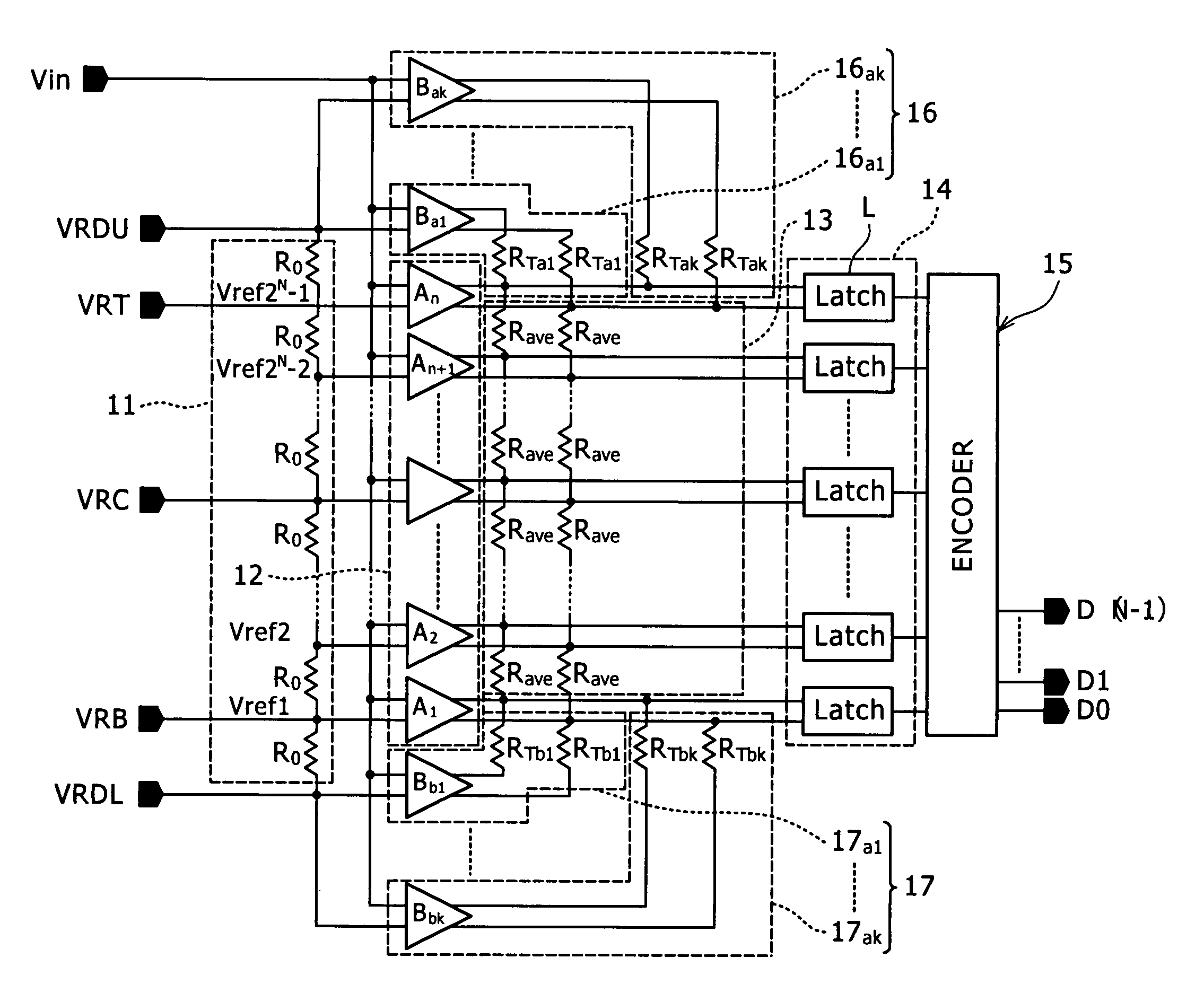
[0029]An AD converter according to the present embodiment is a flash type or parallel type AD converter for which an averaging resistance element is used and is an AD converter of reduced power consumption and a reduced area whose overrange extent is minimized.

[0030]The AD converter according to the present embodiment includes a reference voltage generator for dividing a voltage difference between a first voltage and a second voltage to produce a plurality of reference voltages, a plurality of amplifiers for amplifying difference voltages between the reference voltages and a voltage of an input signal, and a plurality of averaging resistance elements for connecting output terminals of the amplifiers.

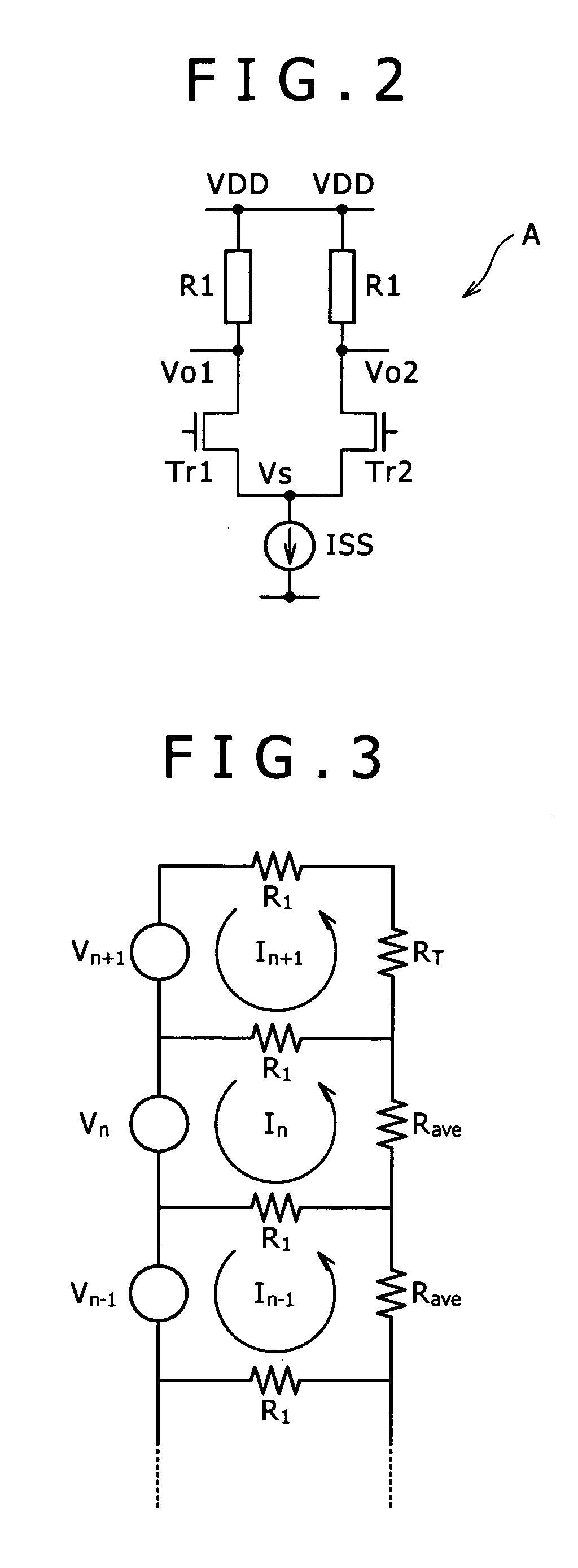
[0031]The AD converter further includes a first averaging auxiliary circuit and a second averaging auxiliary circuit. The first averaging auxiliary circuit includes a first amplifier for amplifying a difference voltage between a third voltage higher than the first voltage and the voltage...


PUM


Abstract

Disclosed herein is an AD converter, including, a reference voltage generator, a plurality of amplifiers, a plurality of averaging resistance elements, and a plurality of first averaging auxiliary circuits each including a first amplifier and a first resistance element.

Description

BACKGROUND OF THE INVENTION[0001]1. Field of the Invention[0002]This invention relates to an AD (analog to digital) converter, and more particularly to an AD converter which includes an averaging resistance element.[0003]2. Description of the Related Art[0004]Commonly, a flash type AD converter (hereinafter referred to simply as “AD converter”) is widely known. While an AD converter of the type described includes a large number of amplifiers for amplifying reference voltages between an input analog signal and different reference voltages, if it is tried to implement a higher resolution, the offset between the amplifiers becomes serious, there is a tendency that the application ranges is limited.[0005]Thus, an AD converter is known wherein an averaging resistance element is provided between outputs of those amplifiers to which reference voltages neighboring with each other are inputted to reduce the offset in order to solve the subject described.[0006]For example, Japanese Patent Lai...

Claims


Application Information

Patent Timeline
Patent Type & Authority Patents(United States)
IPC IPC(8): H03M1/36
CPCH03M1/205H03M1/365
Inventor TOYOMURA, JUNJIINOUE, MIHO
Owner SONY CORP
Why Eureka
Try Eureka