AlGaN/GaN HEMT with normally-off threshold minimized and method of manufacturing the same

a technology of algan/gan hemt and gate recess, which is applied in the direction of semiconductor devices, basic electric elements, electrical appliances, etc., can solve the problems of undesirable variation and off algan/, and achieve the effect of suppressing or minimizing the variation of the threshold voltage (vth)

Inactive Publication Date: 2012-02-14
OKI ELECTRIC IND CO LTD
View PDF2 Cites 12 Cited by
  • Summary
  • Abstract
  • Description
  • Claims
  • Application Information

AI Technical Summary

Benefits of technology

[0007]The present invention was conceived to solve the above-described problems, ant it is therefore an object of the invention to provide a method of forming a gate recess, a method of manufacturing a normally-off AlGaN / GaN-HEMT, and an AlGaN / GaN-HEMT, capable of minimizing variation in the threshold voltage (Vth).
[0009]According to the method of the present invention, the gate recess is formed by photoelectrochemical etching which represents wet etching, while controlling the depth thereof based on the band gap energy of the semiconductor layer to be etched, rather than controlling etching time. Accordingly, the gate recess free from plasma ion-induced damage may be obtained, which would otherwise occur in dry etching.
[0013]In the thus-configured AlGaN / GaN-HEMT, since the UID-AlGaN electron supply layer is an epitaxial layer in which the Al compositional ratio linearly decreases from the interface with the UID-GaN channel layer towards the surface, an appropriate selection of the energy of UV light to be irradiated in the photoelectrochemical etching allows the depth of etching of the gate recess to be set to a desired value.
[0014]According to the present invention, a method of forming a gate recess, a method of manufacturing a normally-off AlGaN / GaN-HEMT, and an AlGaN / GaN-HEMT may be provided, which are capable of suppressing, or at least minimizing, variation in the threshold voltage (Vth).

Problems solved by technology

However, since the gate recess of the normally-off AlGaN / GaN-HEMT of the prior art is formed by dry etching, so that the gate recess may tend to vary in the depth, or may be damaged due to plasma ion, and thereby the threshold voltage (Vth), which is a critical electrical characteristic of the normally-off AlGaN / GaN-HEMT, may undesirably vary.

Method used


Image

  • AlGaN/GaN HEMT with normally-off threshold minimized and method of manufacturing the same
  • AlGaN/GaN HEMT with normally-off threshold minimized and method of manufacturing the same
  • AlGaN/GaN HEMT with normally-off threshold minimized and method of manufacturing the same

Examples


Embodiment Construction

[0020]Now, a preferred embodiment of the present invention will be described in detail with reference to the accompanying drawings. Note that the individual figures are given merely so as to clarify specific features of the present invention, rather than exactly describing all dimensional relations of the individual constituents, and are therefore to be understood that the figures by no means limit the scope of the present invention. Like constituents in the figures are given the same reference numerals.

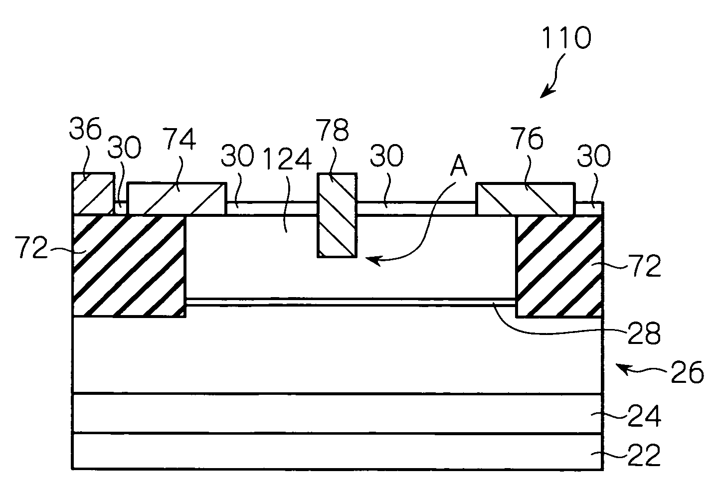
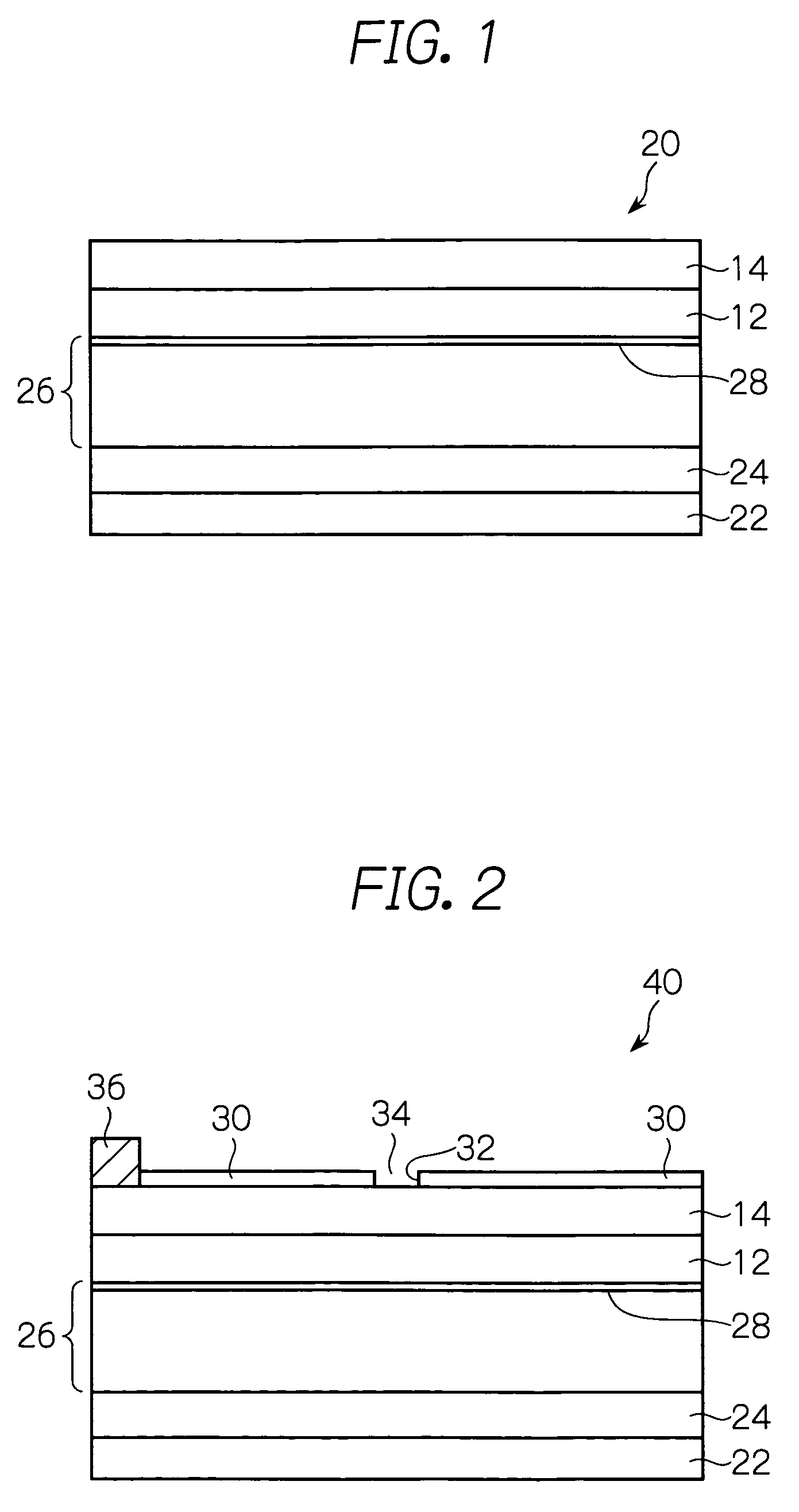
[0021]An illustrative embodiment of the present invention will be described referring to FIGS. 1-6. Firstly, an AlGaN / GaN-HEMT 10 according to the illustrative embodiment of the present invention will be described with reference to FIGS. 1-4.

[0022]As illustrated in FIGS. 1-4, in the AlGaN / GaN-HEMT 110 of the alternative embodiment, a UID-AlGaN electron supply layer has a double-layered structure configured by a UID-AlxGa1-xN layer (x=0.375) 12, which is an AlGaN layer having a substa...


PUM


Abstract

In a method of forming a gate recess, on a surface of an epitaxial wafer including an epitaxial substrate, having a semiconductor layer having the band gap energy varying therein in the depth-wise direction, and a SiN surface protective layer, having a sidewall forming a gate opening and coating the surface of the epitaxial substrate, ultraviolet light having its energy equivalent to the band gap energy of the specific semiconductor layer is irradiated, while the specific semiconductor layer is photoelectrochemically etched from the gate opening with the SiN surface protective layer used as a mask. The gate recess free from plasma ion-induced damage is thus obtained.

Description

BACKGROUND OF THE INVENTION[0001]1. Field of the Invention[0002]The present invention relates to a method of forming a gate recess of a semiconductor device, a method of manufacturing an AlGaN / GaN-HEMT (High-Electron Mobility Transistor), and an AlGaN / GaN-HEMT.[0003]2. Description of the Background Art[0004]A conventional structure and a method of manufacturing an AlGaN / GaN-HEMT, having a recessed-gate structure and normally-off characteristics (enhancement mode), are disclosed in Ken Nakata, et al., “Normally-off AlGaN / GaN HEMT with Recessed Gate for High Power Applications” Technical Report of the Institute of Electronics, Information and Communication Engineers (IEICE), pp. 51-56, ED2005-129, CPM2002-116, LQE005-56, Oct. 2005.[0005]According to the solution, by dry etching such as inductively-coupled plasma reactive ion etching (ICP-RIE), an opening is formed in a SiN surface protective film at a position where a gate electrode is formed later, a gate recess is formed in a UID (U...

Claims


Application Information

Patent Timeline
Patent Type & Authority Patents(United States)
IPC IPC(8): H01L21/336
CPCH01L29/42316H01L29/66462H01L29/7787H01L29/2003
Inventor MARUI, TOSHIHARUOKITA, HIDEYUKI
Owner OKI ELECTRIC IND CO LTD
Why Eureka
Try Eureka