Electromigration resistant via-to-line interconnect

a metal interconnect and electromigration resistance technology, applied in the direction of electrical equipment, semiconductor devices, semiconductor/solid-state device details, etc., can solve the problems of metal line or metal via no longer providing a conductive path in the metal interconnect, product failure of semiconductor devices, metal ions to dislodge from the lattice and move physically, etc., to achieve enhanced electromigration resistance of the metal interconnect structure, impede abrupt electromigration failure, and increase the effect of electromigration resistan

Active Publication Date: 2012-02-14
GLOBALFOUNDRIES U S INC
View PDF9 Cites 7 Cited by
  • Summary
  • Abstract
  • Description
  • Claims
  • Application Information

AI Technical Summary

Benefits of technology

[0014]A liner-to-liner direct contact is formed between the upper metallic liner and the lower metallic liner, which impedes abrupt electromigration failures and enhances electromigration resistance of the metal interconnect structure. The at least one dielectric material portion may include a plurality of dielectric material portions arranged to insure direct contact of between the upper metallic liner and the lower metallic liner. Alternatively, the at least one dielectric material portion may comprise a single dielectric portion of which the area has a sufficient lateral overlap with the area of the conductive via to insure that a liner-to-liner direct contact is formed within the range of allowed lithographic overlay variations. Since the materials of the upper metallic liner and the lower metallic liner have much greater electromigration resistance, the liner-to-liner direct contact has high electromigration resistance and the electrical contact through the liner-to-liner direct contact is maintained even when the interface between the upper metallic liner and the line-level metal portion develops voids, thereby providing enhanced lifetime for the metal interconnect structure.

Problems solved by technology

High defect density, i.e., smaller grain size of the metal, or high temperature typically increases electron scattering, and consequently, the amount of momentum transfer from the electrons to the conductor material.
Such momentum transfer, if performed sufficiently cumulatively, may cause the metal ions to dislodge from the lattice and move physically.
Such a void results in a locally increased resistance in the metal interconnect, or even an outright circuit “open.” In this case, the metal line or the metal via no longer provides a conductive path in the metal interconnect.
Formation of voids in the metal line or the metal via can thus result in a product failure in semiconductor devices.

Method used


Image

  • Electromigration resistant via-to-line interconnect
  • Electromigration resistant via-to-line interconnect
  • Electromigration resistant via-to-line interconnect

Examples


first embodiment

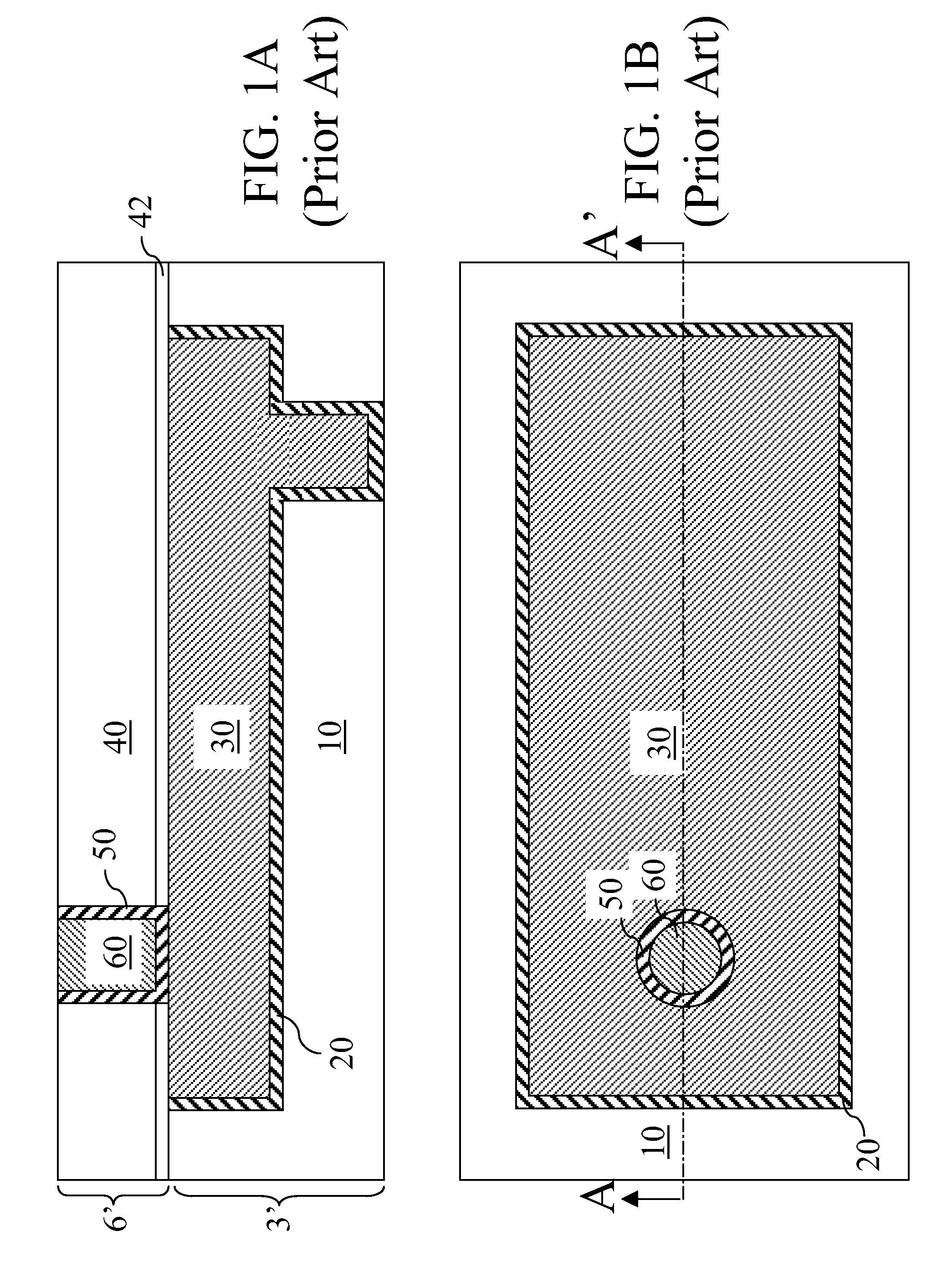
[0039]Referring to FIGS. 3A and 3B, a first exemplary metal interconnect structure according to the present invention comprises a lower dielectric material layer 10 containing a line trench 19, which is a trench formed in the shape of a metal line to be subsequently formed for providing a horizontal electrically conductive path. The line trench 19 may be formed integrally with at least one via cavity 19′ directly connected to a recessed surface 15 of the line trench 19, which is formed below a topmost surface 17 of the lower dielectric material layer 10. A boundary between the line trench 19 and the at least one via cavity 19 is represented by a dotted line in FIG. 3A. A semiconductor substrate (not shown) including at least one semiconductor device may be located beneath the lower dielectric material layer 10. The semiconductor substrate may abut the bottom surface of the lower dielectric material layer 10, or at least one intervening metal interconnect structure (not shown) includ...

seventh embodiment

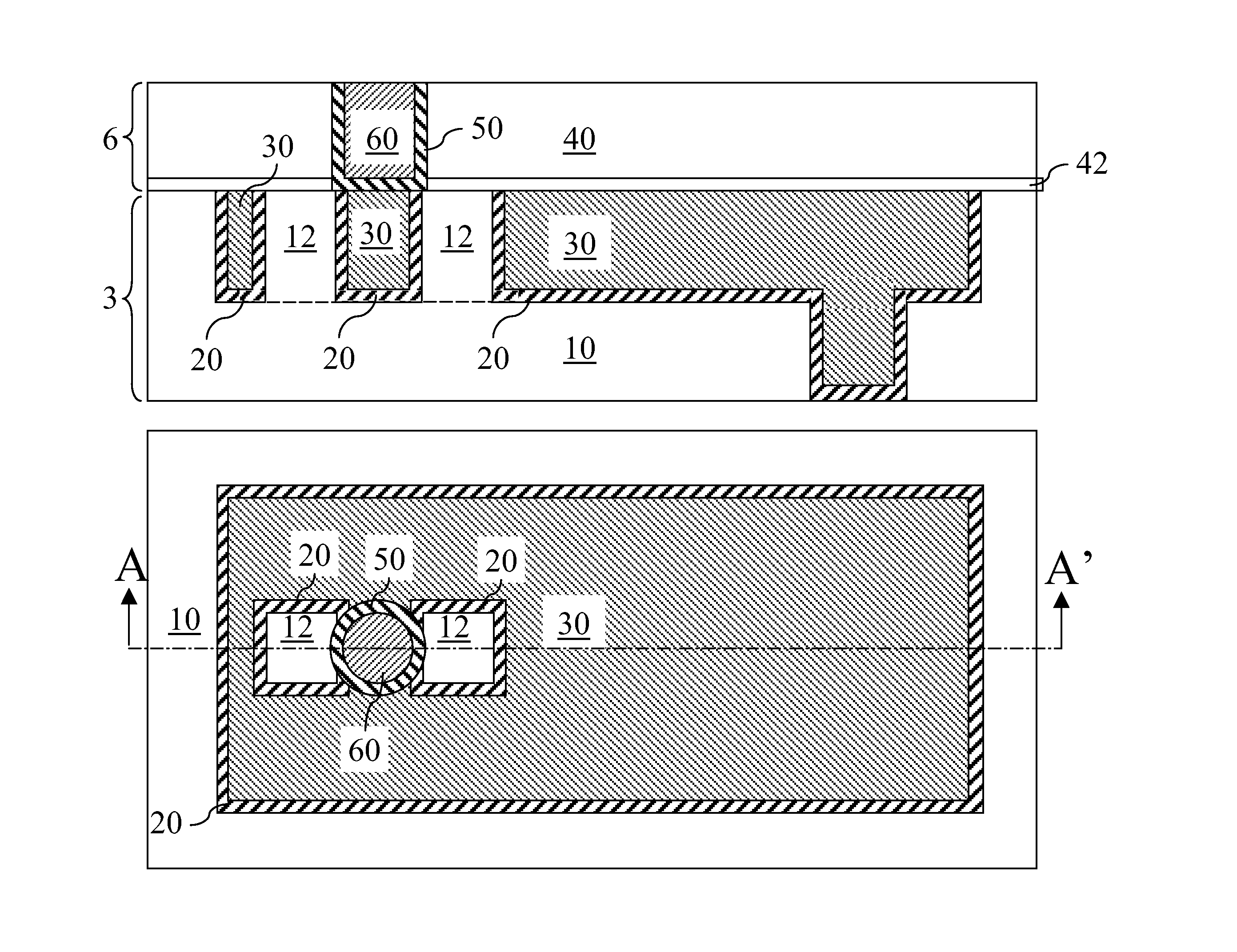
[0085]The maximum distance in the direction connecting the center of mass of the horizontal cross-sectional shape of the conductive via (50, 60) and the center of mass of the cross-sectional shape of the dielectric material portion 12 within the overlap area of the two cross-sectional areas is herein referred to as a lateral overlap distance LOD, which is a measure of the overlay tolerance of the seventh exemplary metal interconnect structure for maintaining a liner-to-liner contact between the upper metallic liner 50 and the lower metallic liner 20. the lateral overlap distance LOD is designed to be greater than maximum lateral overlay variation between the dielectric material portion 12 and the conductive via (50, 60), thereby ensuring the liner-to-liner contact is maintained despite overlay variations during a manufacturing process.

[0086]The current path from the conductive via (50, 60) is in a horizontal direction in the plane of A-A′. The dielectric material portion may be loc...


PUM

PropertyMeasurementUnit
widthaaaaaaaaaa
temperatureaaaaaaaaaa
dielectric constantaaaaaaaaaa

Abstract

A liner-to-liner direct contact is formed between an upper metallic liner of a conductive via and a lower metallic liner of a metal line below. The liner-to-liner contact impedes abrupt electromigration failures and enhances electromigration resistance of the metal interconnect structure. The at least one dielectric material portion may include a plurality of dielectric material portions arranged to insure direct contact of between the upper metallic liner and the lower metallic liner. Alternatively, the at least one dielectric material portion may comprise a single dielectric portion of which the area has a sufficient lateral overlap with the area of the conductive via to insure that a liner-to-liner direct contact is formed within the range of allowed lithographic overlay variations.

Description

FIELD OF THE INVENTION[0001]The present invention relates to metal interconnect structures, and particularly to electromigration resistant metal interconnect structures including a metal line and a conductive via, and methods of manufacturing the same.BACKGROUND OF THE INVENTION[0002]A metal line comprises a lattice of metal ions and non-localized free electrons. The metal ions are formed from metal atoms that donate some of their electrons to a common conduction band of the lattice, and the non-localized free electrons move with relatively small resistance within the lattice under an electric field. Normal metal lines, excluding superconducting materials at or below a superconducting temperature, have finite conductivity, which is caused by interaction of electrons with crystalline imperfections and phonons which are thermally induced lattice vibrations.[0003]When electrical current flows in the metal line, the metal ions are subjected to an electrostatic force due to the charge of...

Claims


Application Information

Patent Timeline
Patent Type & Authority Patents(United States)
IPC IPC(8): H01L21/4763
CPCH01L23/5226H01L21/76816H01L23/528H01L23/5329H01L23/53252H01L23/53238H01L23/53266H01L2924/0002H01L2924/00H01L23/5283H01L21/28
Inventor LI, BAOZHENMCLAUGHLIN, PAUL S.SULLIVAN, TIMOTHY D.
Owner GLOBALFOUNDRIES U S INC
Why Eureka
Try Eureka