
Method and its apparatus for reviewing defects

a defect inspection and defect technology, applied in the field of methods and their apparatus for reviewing defects, can solve the problems of increasing the number of defects to be reviewed per wafer, preventing erroneous detection, and inability to discriminate in detail in most cases, so as to improve the detection ratio, reduce the number of defects to be reviewed, and reduce the effect of erroneous detection

Inactive Publication Date: 2012-02-21
HITACHI HIGH-TECH CORP
View PDF11 Cites 7 Cited by
  • Summary
  • Abstract
  • Description
  • Claims
  • Application Information

AI Technical Summary

Benefits of technology

The invention provides a method and apparatus for reviewing defects in semiconductor devices using a scanning electron microscope. The method involves imaging the defect in low magnification, synthesizing a reference image from the low magnification image, and extracting the defect applicant. The apparatus includes scanning electron microscope means, low magnification defect image acquisition means, reference image synthesis means, and enlarged image acquisition means. The technical effect of the invention is to provide a high through-put method for reviewing defects in semiconductor devices.

Problems solved by technology

Though the approximate feature of the defect can be grasped by confirming the existence of the defect from the detected images of low resolution, the kind of the defect cannot be discriminated in detail in most cases.
The problem that arises hereby is an error between the defect coordinates outputted by the defect inspection apparatus and actual defect coordinates.
As an aperture ratio of semiconductor wafers has become greater in recent years, the number of defects to be reviewed per wafer has increased, too.
However, this results in the increase of the processing time of the defect detection processing because a long processing time is generally necessary for calculating feature quantities from images.

Method used


Image

  • Method and its apparatus for reviewing defects
  • Method and its apparatus for reviewing defects
  • Method and its apparatus for reviewing defects

Examples


embodiment 1

[0039]A semiconductor wafer defect reviewing apparatus (review SEM) using a scanning electron microscope will be explained as a first embodiment of the invention.

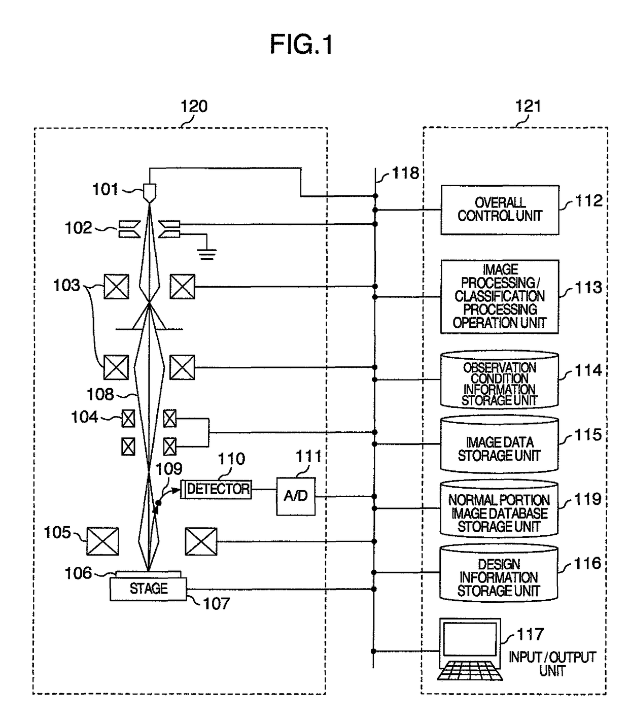
[0040]FIG. 1 shows an apparatus construction of the review SEM according to the invention. The review SEM according to the invention includes an SEM image acquisition unit 120 and a signal processing unit 121 that are connected to one another through buses 118. Reference numeral 101 in the SEM image acquisition unit 120 denotes an electron source for generating primary electrons 108, reference numeral 102 denotes an acceleration electrode for accelerating the primary electrons, reference numeral 103 denotes a convergent lens for converging the primary electrons, reference numeral 104 denotes a deflector for scanning and deflecting two-dimensionally the primary electrons and reference numeral 105 denotes an objective lens for converging the primary electrons onto a sample 106. Reference numeral 107 denotes a stage capable of...

embodiment 2

[0071]A review system having the same hardware construction as that of the first embodiment and the ADR processing function shown in FIG. 2 will be explained as Embodiment 2.

[0072]The first embodiment represents the method that automatically generates the normal portion image database by executing the ADR processing for generating the normal portion image database. A method for automatically generating the normal portion image database on the basis of design information of semiconductors will be hereinafter explained with reference to FIG. 9.

[0073]In the construction of the review SEM shown in FIG. 1, the operation unit 113 analyzes the geometric information of the circuit pattern imaged by the SEM image acquisition unit 120 from the design information of the semiconductor devices stored in the storage unit 116 and extracts the coordinates of the peculiar portion existing inside the region having periodicity (S901). Next, when the peculiar portion is judged as existing as a result o...


PUM


Abstract

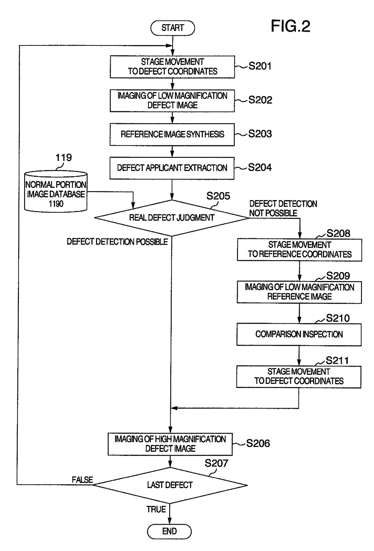
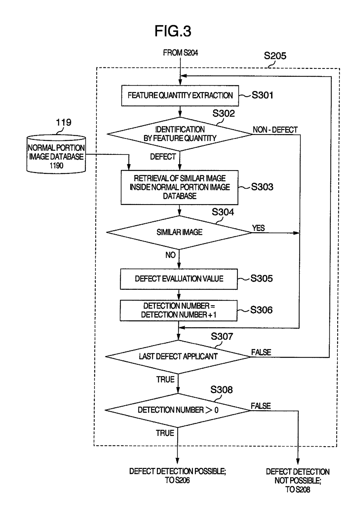
A method for reviewing a defect on a sample involves the steps of imaging a defect image containing the defect in first magnification by using an image acquisition unit, synthesizing a reference image not containing the defect from the defect image, comparing the defect image acquired with the reference image synthesized to detect a defect applicant, executing a processing for classifying the defect applicant into a defect and a normal portion and imaging only the portion identified as the detect in second magnification. The method makes it possible to specify a defect position without error from the image taken in the first magnification and to image the defect in the second magnification when a large number of defects are observed within a short time by using the image acquisition unit.

Description

INCORPORATION BY REFERENCE[0001]The present application claims priority from Japanese application JP 2008-095657 filed on Apr. 2, 2008, the content of which is hereby incorporated by reference into this application.BACKGROUND OF THE INVENTION[0002]This invention relates to a method and its apparatus for reviewing defects on a sample by using image acquisition means.[0003]To improve production yield in the manufacture of semiconductor devices, it has been of importance to quickly clarify the cause of occurrence of defects in the manufacturing process. A defect inspection apparatus and a defect reviewing apparatus have now been used in combination at present in the actual scene of the manufacture to analyze the defects. The defect inspection apparatus is the one that inspects semiconductor wafer to detect defects by using optical means or electron beams and outputs feature quantities of the defects detected and their coordinate information.[0004]It is important for the defect inspecti...

Claims


Application Information

Patent Timeline
Patent Type & Authority Patents(United States)
IPC IPC(8): G06K9/00
CPCG06K9/033G06T7/001G06K2209/19G06T2207/10056G06T2207/30148G06V10/987G06V2201/06
Inventor HARADA, MINORUNAKAGAKI, RYOOBARA, KENJI
Owner HITACHI HIGH-TECH CORP
Learn More