
Metal material and its manufacturing method, thin-film device and its manufacturing method, element-side substrate and its manufacturing method, and liquid crystal display and its manufacturing method

a technology of metal materials and manufacturing methods, applied in the direction of optical elements, instruments, transportation and packaging, etc., can solve the problems of deteriorating the optical performance of the liquid crystal display apparatus, increasing the number of manufacturing steps, etc., to prevent an electrical corrosion, eliminate or reduce the difference of work functions, and excellent image quality

Inactive Publication Date: 2012-02-28
SHARP KK
View PDF8 Cites 0 Cited by
  • Summary
  • Abstract
  • Description
  • Claims
  • Application Information

AI Technical Summary

Benefits of technology

This approach enhances image quality by minimizing display flicker and maintaining optical performance without increasing manufacturing steps, while improving the reliability of the liquid crystal display by reducing the difference in direct current offset voltages between electrodes.

Problems solved by technology

Therefore, a problem of increasing the number of the manufacturing steps occurs.
In addition, since a film is laminated on the reflective electrode, a problem of deteriorating the optical performance of the liquid crystal display apparatus occurs.

Method used


Image

  • Metal material and its manufacturing method, thin-film device and its manufacturing method, element-side substrate and its manufacturing method, and liquid crystal display and its manufacturing method
  • Metal material and its manufacturing method, thin-film device and its manufacturing method, element-side substrate and its manufacturing method, and liquid crystal display and its manufacturing method
  • Metal material and its manufacturing method, thin-film device and its manufacturing method, element-side substrate and its manufacturing method, and liquid crystal display and its manufacturing method

Examples


Embodiment Construction

[0092]Hereinafter, a case will be described in detail with reference to the accompanying drawings, in which an embodiment of a metal material according to the present invention having the work function thereof controlled by changing by at least a predetermined value by a plasma treatment and a method for manufacturing the metal material; and a thin-film device using the metal material for a metal thin film material and a method for manufacturing the thin-film device is applied to an element-side substrate, a semi-transmissive reflective liquid crystal display apparatus using a method for manufacturing the element-side substrate, and a method for the semi-transmissive reflective liquid crystal display apparatus.

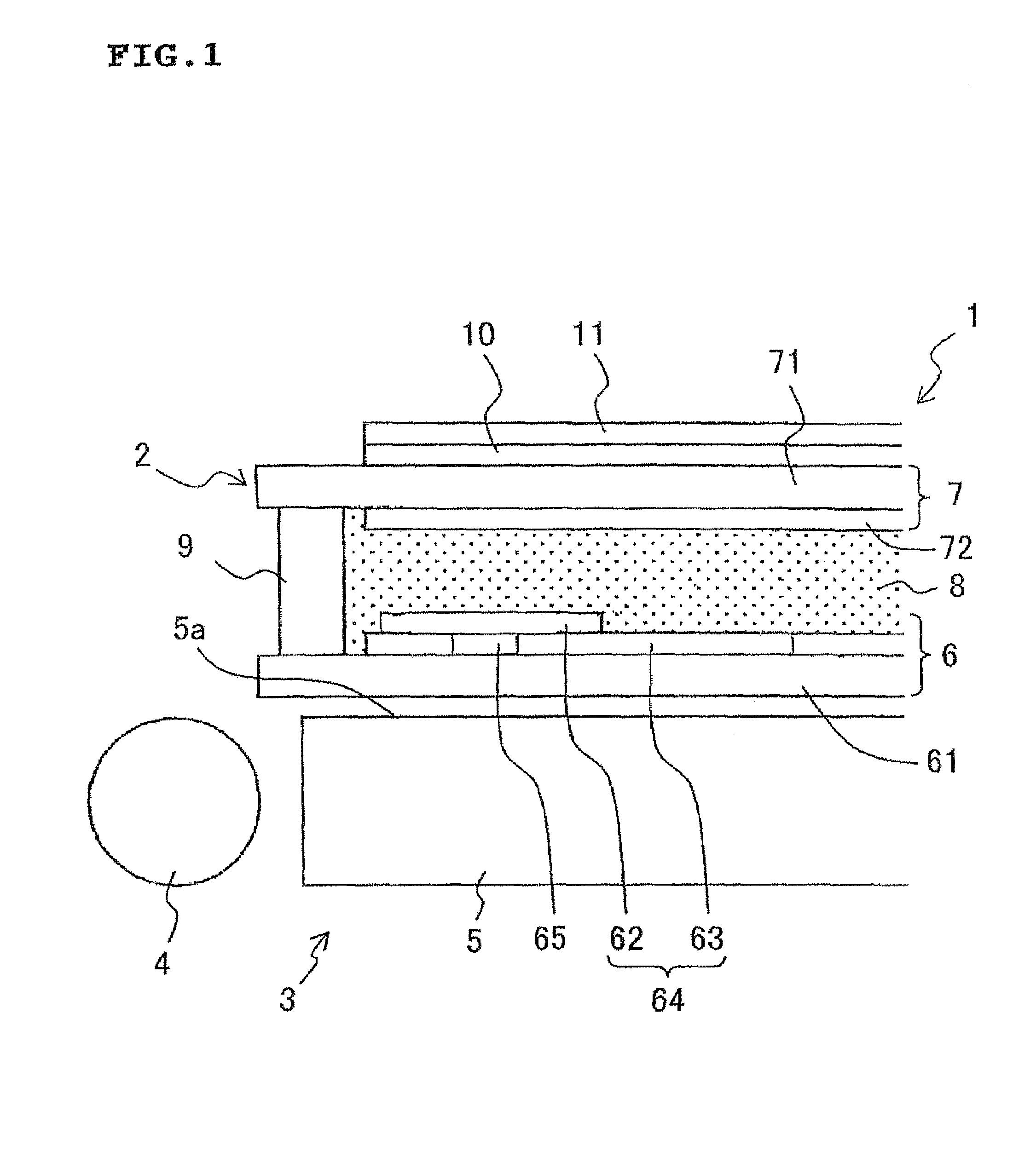
[0093]FIG. 1 is a cross-sectional view showing an exemplary structure of a semi-transmissive reflective liquid crystal display apparatus 1 according to an embodiment of the present invention.

[0094]In FIG. 1, the semi-transmissive reflective liquid crystal display apparatus 1 h...


PUM

PropertyMeasurementUnit
pressureaaaaaaaaaa
work functionaaaaaaaaaa

Abstract

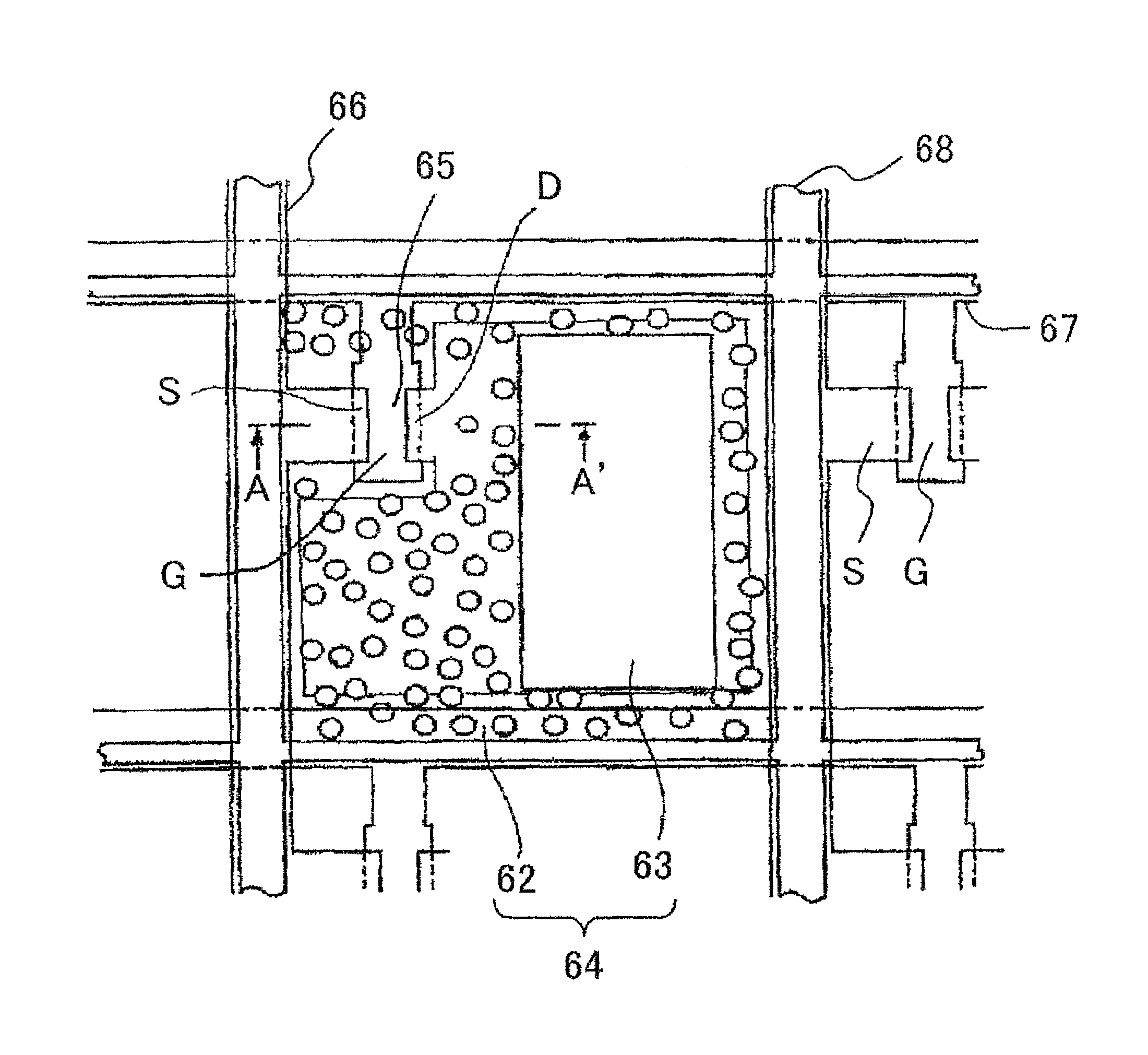
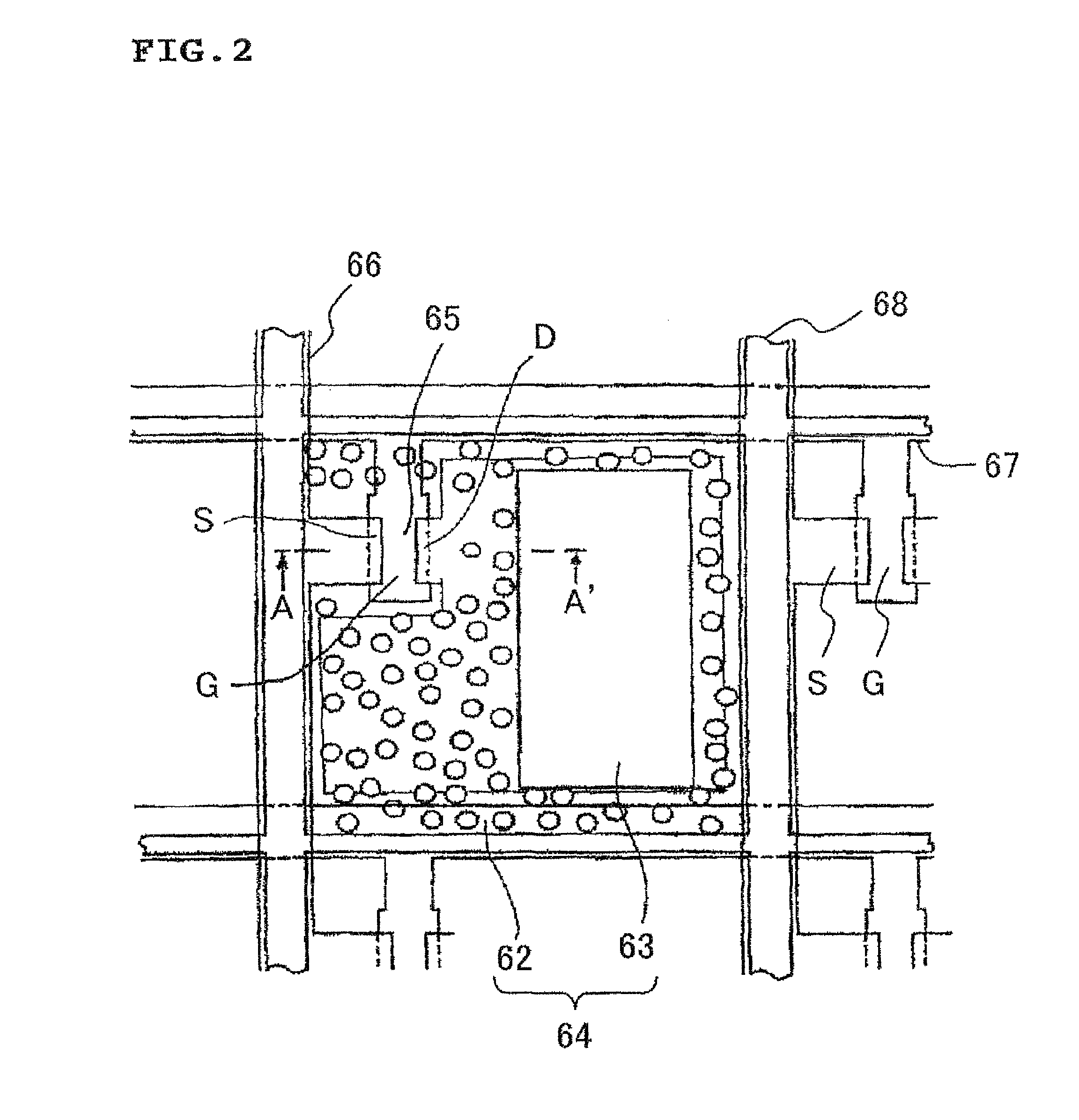
A difference of work functions in different metal thin films is suppressed without causing the increase of the manufacturing steps or the decrease of the optical performance. In a semi-transmissive reflective liquid crystal display apparatus 1 including a reflective electrode 62 and a transmissive electrode 63 in the pixel electrode 64, the surface of the reflective electrode 62 is subject to a plasma treatment, so that the work function of the reflective electrode 62 is controlled by changing by a value of 0.1 eV from the original value. Thus, it is possible to place the work function of the reflective electrode 62 within a difference of ±0.2 eV with respect to the work function of the transmissive electrode 63. As a result, a number of the manufacturing steps is not increased or no optical performance is decreased, unlike conventional liquid crystal display apparatuses. Even if the optimum direct current offset voltage is applied to one of the reflective electrode 62 and the transmissive electrode 63, it is possible to reduce the deterioration of an image display quality resulting from the difference with the optimum direct current offset voltage for the other electrode. As such, it is possible to improve the display quality of the liquid crystal display apparatus 1.

Description

[0001]This application is the U.S. national phase of International Application No. PCT / JP2006 / 303332, filed 23 Feb. 2006 which designated the U.S. and claims priority to Japanese Patent Application No. 2005-064605, filed 8 Mar. 2005, the entire contents of each of which are hereby incorporated by reference.TECHNICAL FIELD[0002]The present invention relates to: a metal material and a method for manufacturing the metal material; a thin-film device using the metal material for a metal thin film material and a method for manufacturing the thin-film device; an element-side substrate including a reflective section for producing a reflective display using surrounding light as an illumination, the reflective section including the metal material for a reflective metal electrode, and a transmissive section for producing a transmissive display using backlight as an illumination in one pixel and a method for manufacturing the element-side substrate; and a semi-transmissive reflective liquid cry...

Claims


Application Information

Patent Timeline
Patent Type & Authority Patents(United States)
IPC IPC(8): G02F1/1343
CPCC23F4/00G02B5/0808G02F1/133555H01L29/458H01L29/66765H01L27/124G02F1/13439Y10T428/12493
Inventor FUJITA, TETSUOKOKURA, MASAFUMIHARADA, MITSUNORINAKAHARA, HIJIRIKATAOKA, YOSHIHARU
Owner SHARP KK
Learn More