Devices with faraday cages and internal flexibility sipes

a technology of internal flexibility and faraday cages, which is applied in the direction of electrical apparatus contruction details, electrical apparatus casings/cabinets/drawers, instruments, etc., can solve the problems of inability to overcome, no products were released, inherent flaws of semiconductor wafers, etc., and achieve the effect of reducing their rol

Active Publication Date: 2012-02-28
ELLIS
View PDF22 Cites 51 Cited by
  • Summary
  • Abstract
  • Description
  • Claims
  • Application Information

AI Technical Summary

Benefits of technology

[0022]Second, the applicant's disclosure solves the longstanding unequal thermal expansion problem discussed above by reducing, even almost eliminating the need for pins, since both on wafer and off wafer communication by the independently functioning microchips (personal computer SoC's) on the wafer can be accomplished by radio or optics connections that do not require pins or require far fewer structural connections. In addition, the applicant's use of stacked semiconductor wafers, which can have very similar or identical materials and expansion rates, can obviate the need for conventional motherboards or reduce their role.
[0023]Moreover, since the personal computer microchips on the semiconductor wafer can operate independently, such as in conventional clusters of several or many or all of the personal computers on the wafer (or including personal computers off the wafer as well), the operations occurring on the wafer can be asynchronous. The applicant's disclosure thereby also solves the longstanding problem of synchronizing such wafer scale operations by obviating the need for synchronizing them, as would be necessary without the applicant's disclosure.

Problems solved by technology

Many companies including TI and ITT attempted to develop “wafer scale integration” (WSI) production systems in the 1970's and ‘80’s, but all failed and no products were released.
One critical problem that has not been overcome is that of inherent flaws in semiconductor wafers.
There were several subsequent efforts in the 1980's, but none successful.
Another well-known problem is the field of wafer-scale integration technology is the impact of thermal expansion on external connectivity.
More specifically, when a WSI microelectronic complex is connected to a circuit board by thousands of, for example, connectors positioned between the microelectronic complex and the circuit board, these connectors can be damaged due to the different rates of thermal expansion experience by the surfaces of the microelectronic comples and circuit board.
Thus, as the two materials heat up, the two surfaces will expand at different rates, potentially damaging many of the connectors distributed between the wafer and the circuit board.
In addition, the applicant's use of stacked semiconductor wafers, which can have very similar or identical materials and expansion rates, can obviate the need for conventional motherboards or reduce their role.

Method used


Image

  • Devices with faraday cages and internal flexibility sipes
  • Devices with faraday cages and internal flexibility sipes
  • Devices with faraday cages and internal flexibility sipes

Examples


Embodiment Construction

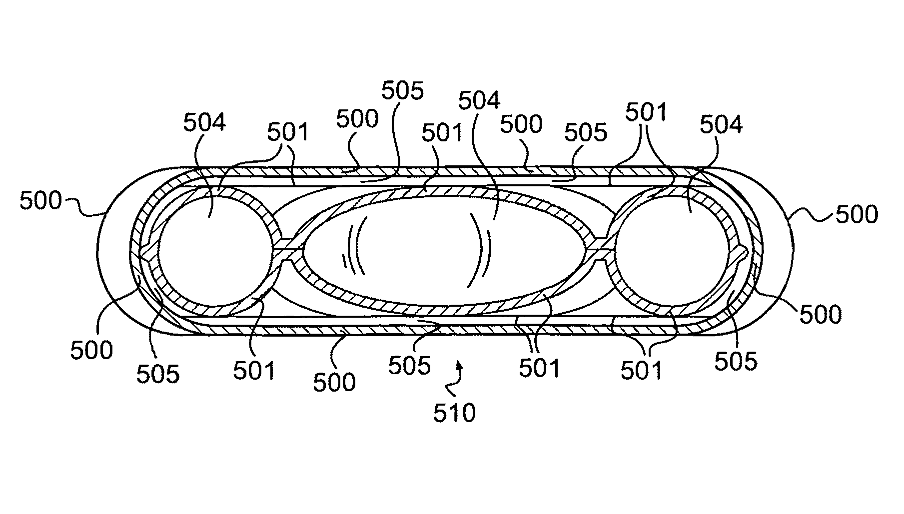
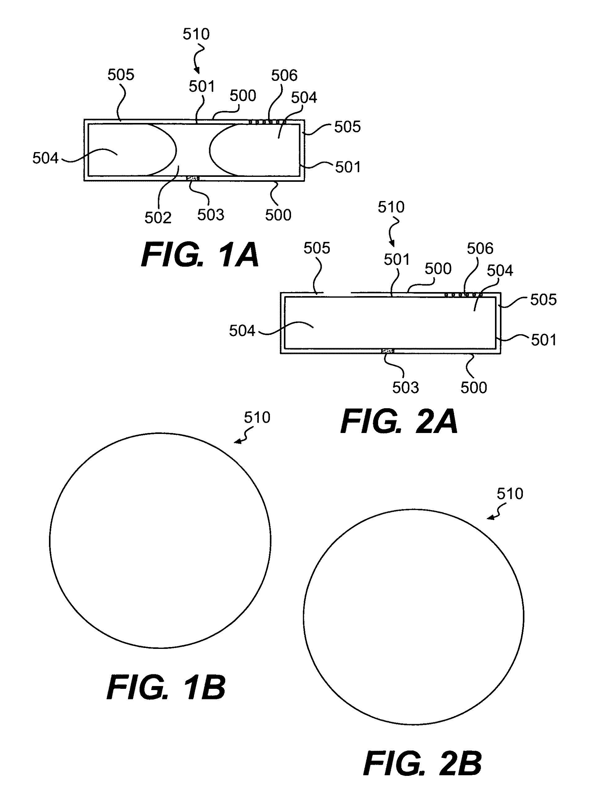
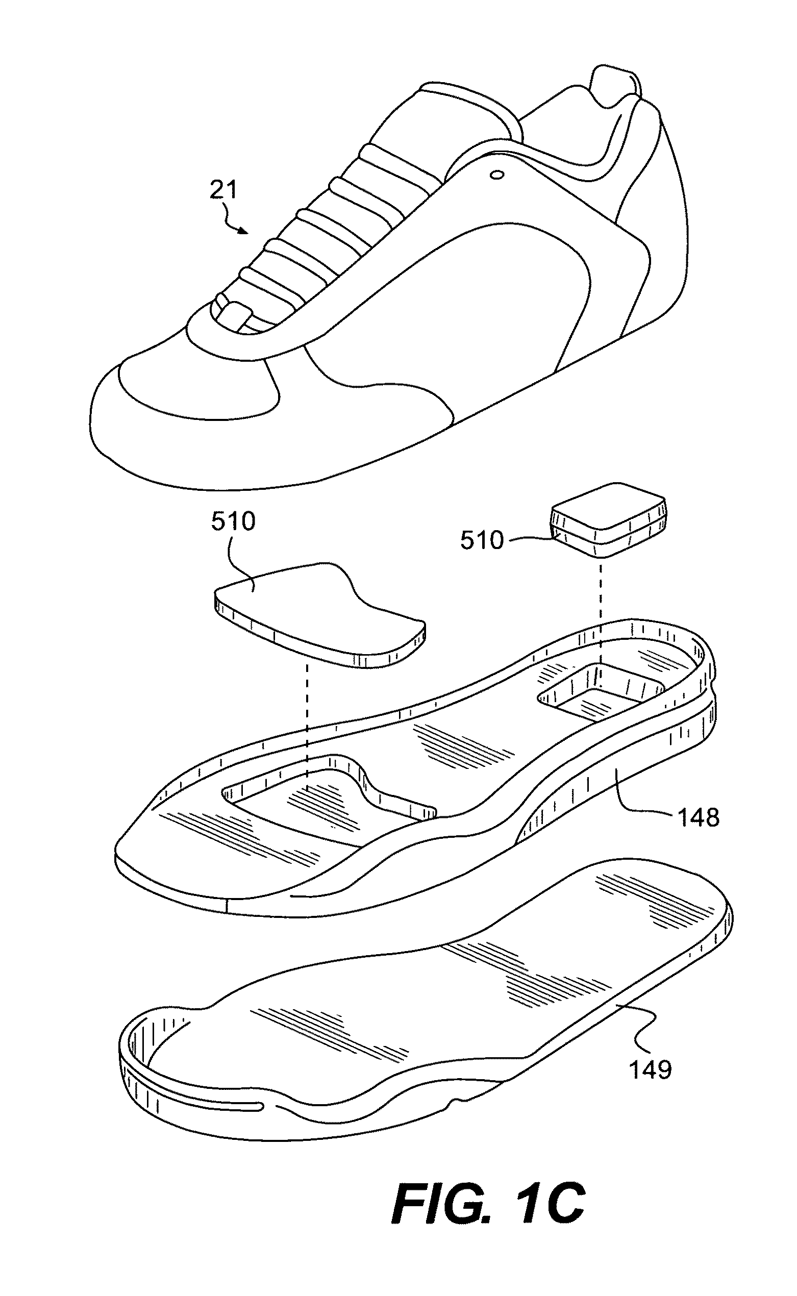
[0056]FIGS. 1-9 of this application are FIGS. 1-6, 52, 61, 67, 74, and 79 of both the applicant's U.S. application Ser. No. 11 / 802,033 filed May 18, 2007 and published on Apr. 10, 2008 as Pub. No. US 2008 / 0083140 A1 and PCT Application PCT / US2007 / 011976 filed 18 May 2007 and published on 31 Jan. 2008 as Int. Pub. No. WO 2008 / 013594 A2, as well as U.S. application Ser. No. 11 / 802,930 filed May 25, 2007 and published on Apr. 17, 2008 as Pub. No. US 2008 / 0086916 A1; all three applications are incorporated herein by reference. In addition, FIGS. 1-6 (except 6D-6F) of this application are FIGS. 83-88 of both the applicant's U.S. application Ser. No. 11 / 282,665 filed Nov. 21, 2005 and published on Nov. 9, 2006 as Pub. No. US 2006 / 0248749 A1 and PCT Application PCT / US2005 / 042341 filed 21 Nov. 2005 and published on 1 Jun. 2006 as Int. Pub. No. WO 2006 / 058013 A2, both of which are incorporated herein by reference.

[0057]FIGS. 1-9 show the applicant's prior inventions incorporating forms of in...


PUM


Abstract

A computer or microchip comprising an outer chamber and at least one inner chamber inside the outer chamber. The outer chamber and the inner chamber being separated at least in part by an internal sipe, and at least a portion of a surface of the outer chamber forming at least a portion of a surface of the internal sipe. The internal sipe has opposing surfaces that are separate from each other and therefore can move relative to each other, and at least a portion of the opposing surfaces are in contact with each other in a unloaded condition. The outer chamber including a Faraday Cage. A computer, comprising an undiced semiconductor wafer having a multitude of microchips. The multitude of microchips on the wafer forming a plurality of independently functioning computers, each computer having independent communication capabilities.

Description

[0001]This application is a continuation-in-part of prior application Ser. No. 12 / 292,553, filed Nov. 20, 2008, which claims the benefit of U.S. Provisional Application No. 60 / 996,530, filed on Nov. 21, 2007. This application also claims the benefit of U.S. Provisional Application No. 60 / 996,553, filed on Nov. 26, 2007.BACKGROUND[0002]1. Field of the Disclosure[0003]The disclosure relates to a Faraday Cage surrounding semiconductor microchips, photovoltaic cells, and / or other micro and / or nano devices combined with the applicant's prior internal sipe inventions, including at least one compartment surrounded by at least one internal sipe, such as a slit. More specifically, a Faraday Cage coincides with an outer compartment, which forms one surface of a sipe surrounding an inner compartment including a personal computer microchip and / or a photovoltaic cell and / or a fuel cell and / or a battery.[0004]The disclosure also relates to a semiconductor wafer, such as silicon, containing a mult...

Claims


Application Information

Patent Timeline
Patent Type & Authority Patents(United States)
IPC IPC(8): G06F1/20H05K9/00
CPCA43B3/0005H01L23/552H01L25/16G06F1/182G06F1/20H05K9/0024H05K9/0049H04L63/02H01L23/60G06F1/16H01L2924/0002H01L2924/00A43B3/34
Inventor ELLIS, FRAMPTON E.
Owner ELLIS
Why Eureka
Try Eureka