Apparatus and method for recycling the energy from load capacitance
a load capacitance and apparatus technology, applied in the direction of electric variable regulation, process and machine control, instruments, etc., can solve the problems of reducing the power saved by voltage reduction, reducing the efficiency of load capacitance, and consuming a large amount of power, etc., to achieve rapid and accurate voltage restoration, raise and lower voltages, and unprecedented speed and accuracy
- Summary
- Abstract
- Description
- Claims
- Application Information
AI Technical Summary
Benefits of technology
Problems solved by technology
Method used
Image
Examples
example 1
Flyback Amplifier with Bidirectional Agility
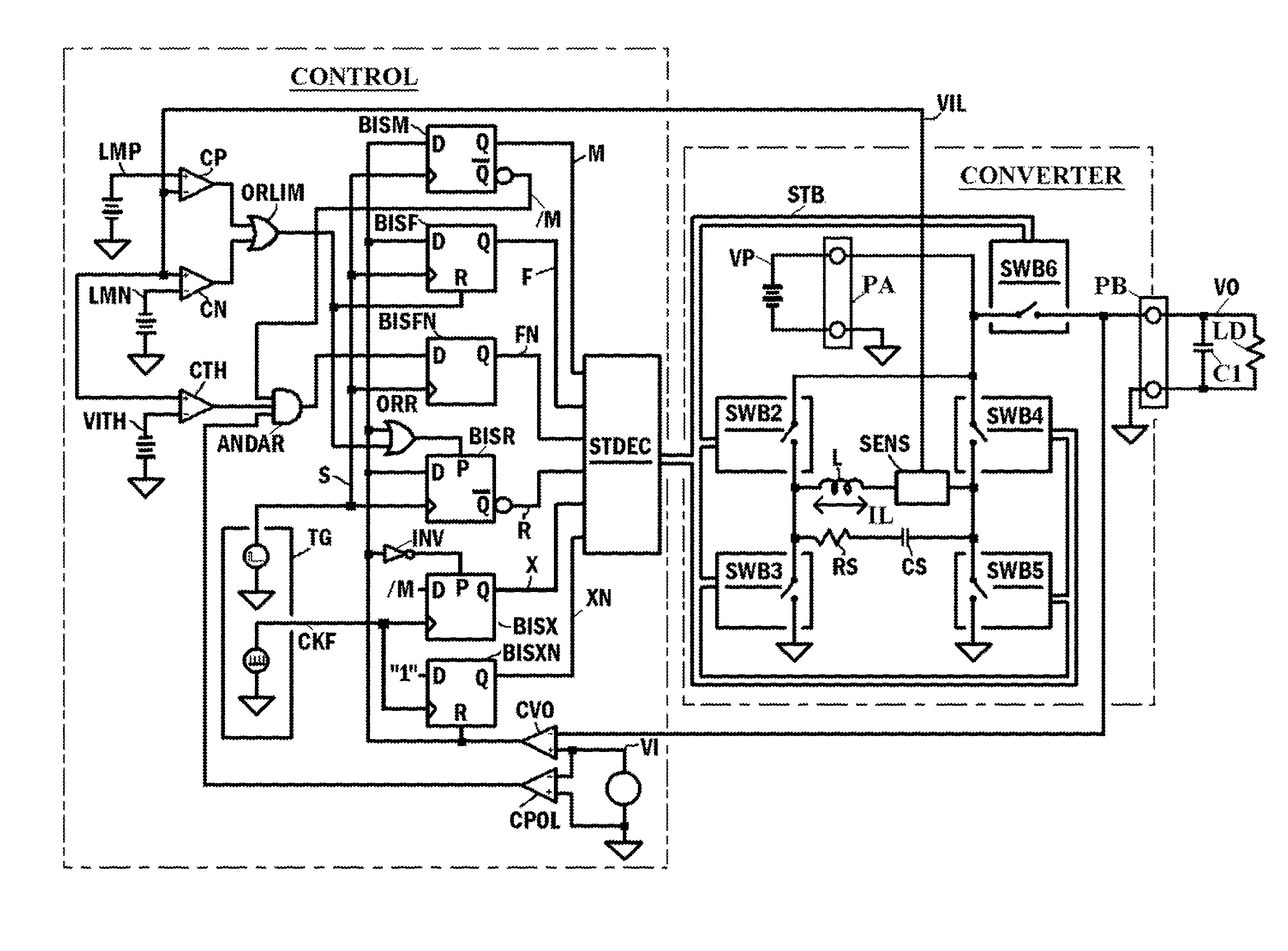
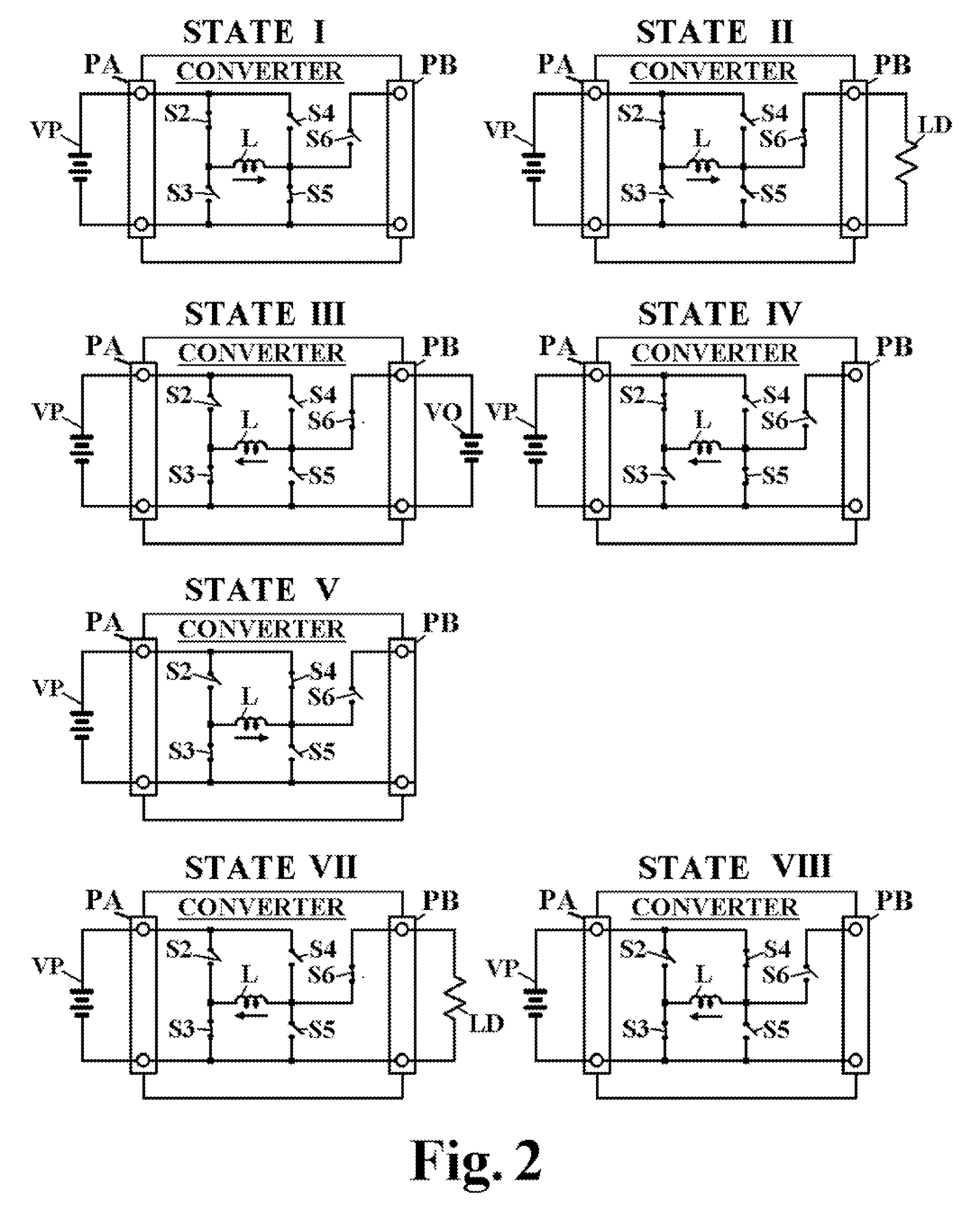
[0032]FIG. 3 depicts a state decoder STDEC for generating the States I through VIII of FIG. 2 responsive to the outputs of flip-flops to be shown below in FIG. 24 in accordance with the following logical expressions:
State I=M&F
State II=M& / F& / X
State III= / M&R& / FN
State IV= / M& / R& / FN| / M& / R&FN& / XN
State V=M& / F&X
State VII= / M& / R&FN&XN
State VIII= / M&R&FN
where the signals cited correspond to those illustrated in FIGS. 3 and 5, and to the like-named States of FIG. 2, and
[0033]“&” represents the logical AND function,
[0034]“|” represents the logical OR function,[0035]the prefix “ / ” performs the logical NOT upon its suffix.
[0036]For convenience of description the outputs of STDEC are shown as a state bus STB of digital signals.
[0037]FIG. 4 shows switch-block SWBn, which is the embodiment of a single switch of FIG. 2. It is to be understood that the n of SWBn is to be a digit, here 2 through 6, representing an instance of SWBn corresponding to S2 through S...
example 2
Simplified Buck Converter Adapted for Capacitive Energy Recovery
[0063]FIG. 9 shows a simplified converter according to the present invention, which is capable of useful capacitive energy recovery, but is not agile like the full embodiment of example 1.
[0064]A signal RUN is provided by a switch SRUN, shown connected to a logical 1, which control signal may be provided by an external source. When RUN is asserted, the converter forms a buck converter.
[0065]Switches S2 and S3, usually MOSFETs, form a totem pole switch for the buck converter supplied through port PA from power input VP. DS2 and DS3 represent the body diodes of their respective FET switches, those switches shown here in idealized form. L is the switched inductor. Attached to port PB is a load LD comprising a substantially non-reactive current sink and a capacitor C1. C1 represents the aggregate of filter and bypass capacitors in shunt with the load. IGBT's, BJT's, or magnetic amplifiers may also be used as switches. Indee...
PUM
 Abstract
Description
Claims
Application Information


