

Head substrate, printhead, head cartridge, and printing apparatus
a head substrate and cartridge technology, applied in printing and other directions, can solve the problems of difficult to design the gate width of the driver transistor integrated in the head substrate with a margin for characteristics, and increasing the chip size on a head substrate having a nozzle density of 1,200 dpi. , to achieve the effect of suppressing the influence of heat of the heater on the discharge characteristic of the transistor,
- Summary
- Abstract
- Description
- Claims
- Application Information
AI Technical Summary
Benefits of technology
Problems solved by technology
Method used
Image

Examples
first embodiment
[0089]FIG. 4 is a block diagram showing the layout of a head substrate according to the first embodiment of the present invention.
[0090]In FIG. 4, the same reference numerals as those described above denote the same parts, and a description thereof will not be repeated. In FIG. 4, reference numeral 103′ denotes a transistor array; 104a′, a logic circuit.
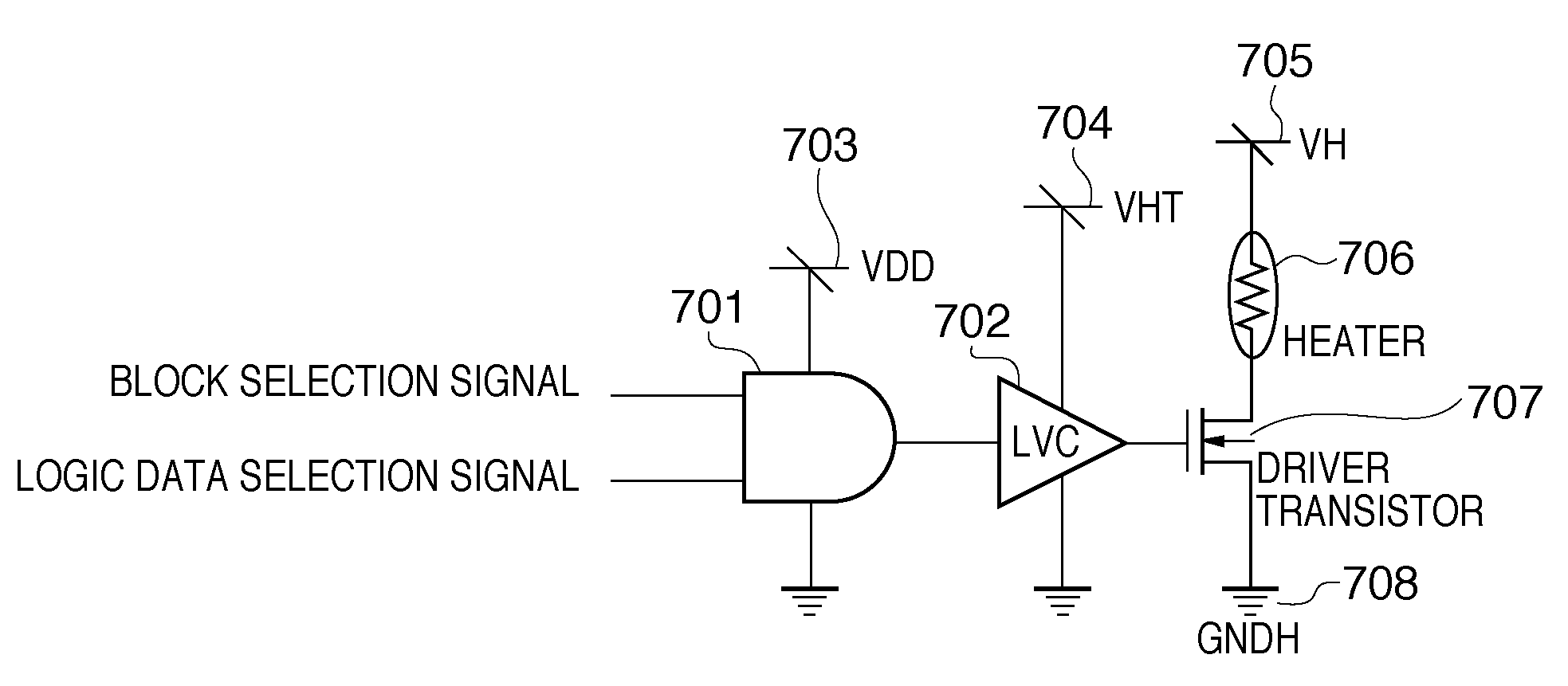
[0091]FIG. 5 is a block diagram for explaining a series of operations until the heater is driven after inputting print data to the head substrate. In FIG. 5, the signal flow is schematically indicated by arrows. FIG. 5 shows a circuit block corresponding to one ink supply port.
[0092]In FIG. 5, the same reference numerals as those described above denote the same parts, and a description thereof will not be repeated. In FIG. 5, reference numeral 104a′ denotes a logic circuit including an AND circuit and voltage conversion circuit referred to with reference to FIG. 10.
[0093]FIG. 6 is a plan view showing the layout of the head substrate ...
second embodiment
[0099]FIG. 15 is a plan view of a layout for explaining the second embodiment of the present invention.
[0100]In FIG. 15, the same reference numerals as those shown in FIG. 6 denote the same parts. In this arrangement, a driver transistor 103a and logic circuit 104a′ are interchanged, as described in the first embodiment. In addition, heaters are arranged at double the density in FIG. 6.
[0101]In the conventional arrangement, when the nozzle density increases to about 1,200 dpi which is double the density of 600 dpi, the number of gates per nozzle decreases to two at 1,200 dpi though four driver transistor gates can be arranged per nozzle at 600 dpi. Only driver transistors having half the gate width W at 600 dpi can be formed in a transistor region of the same area. As a result, driver transistors cannot be designed with a margin for the gate width W, and a change of the ON resistance under the influence of heat generated by the heater may influence the discharge characteristic. When...
third embodiment
[0104]FIG. 7 is a block diagram showing the layout of a head substrate according to the third embodiment of the present invention.
[0105]In FIG. 7, the same reference numerals as those described above denote the same parts, and a description thereof will not be repeated. In FIG. 7, reference numeral 106 denotes an empty space.
[0106]In addition to the arrangement in the first embodiment, a feature of the third embodiment is that driver transistors are arranged at a pitch smaller than the heater pitch to newly create the empty spaces 106 hatched in FIG. 7.
[0107]FIG. 8 is a plan view showing the layout of the head substrate shown in FIG. 7.
[0108]In FIG. 8, the same reference numerals as those described above denote the same parts.
[0109]In the conventional arrangement, if the heater pitch and driver transistor pitch are set different from each other, like the third embodiment, a predetermined distance needs to be set to lay out diagonal wiring in order to connect heaters and driver trans...
PUM
 Abstract
Description
Claims
Application Information