Method of making 3D integrated circuits

a technology of integrated circuits and components, applied in the direction of semiconductor devices, semiconductor/solid-state device details, electrical apparatus, etc., can solve the problems of minimum size needed to make these components, physical limits of the density that can be achieved in two dimensions, and the requirement of more complex designs

Active Publication Date: 2012-04-17
GLOBALFOUNDRIES US INC
View PDF61 Cites 223 Cited by
  • Summary
  • Abstract
  • Description
  • Claims
  • Application Information

AI Technical Summary

Problems solved by technology

Although dramatic improvements in lithography have resulted in considerable improvements in 2D integrated circuit formation, there are physical limits to the density that can be achieved in two dimensions.
One of these limits is the minimum size needed to make these components.
Also, when more devices are put into one chip, more complex designs are required.
An additional limitation comes from the significant increase in the number and length of interconnections between devices as the number of devices increases.
When the number and length of interconnections increase, both circuit resistance-capacitance (RC) delay and power consumption increase.

Method used


Image

  • Method of making 3D integrated circuits
  • Method of making 3D integrated circuits
  • Method of making 3D integrated circuits

Examples


Embodiment Construction

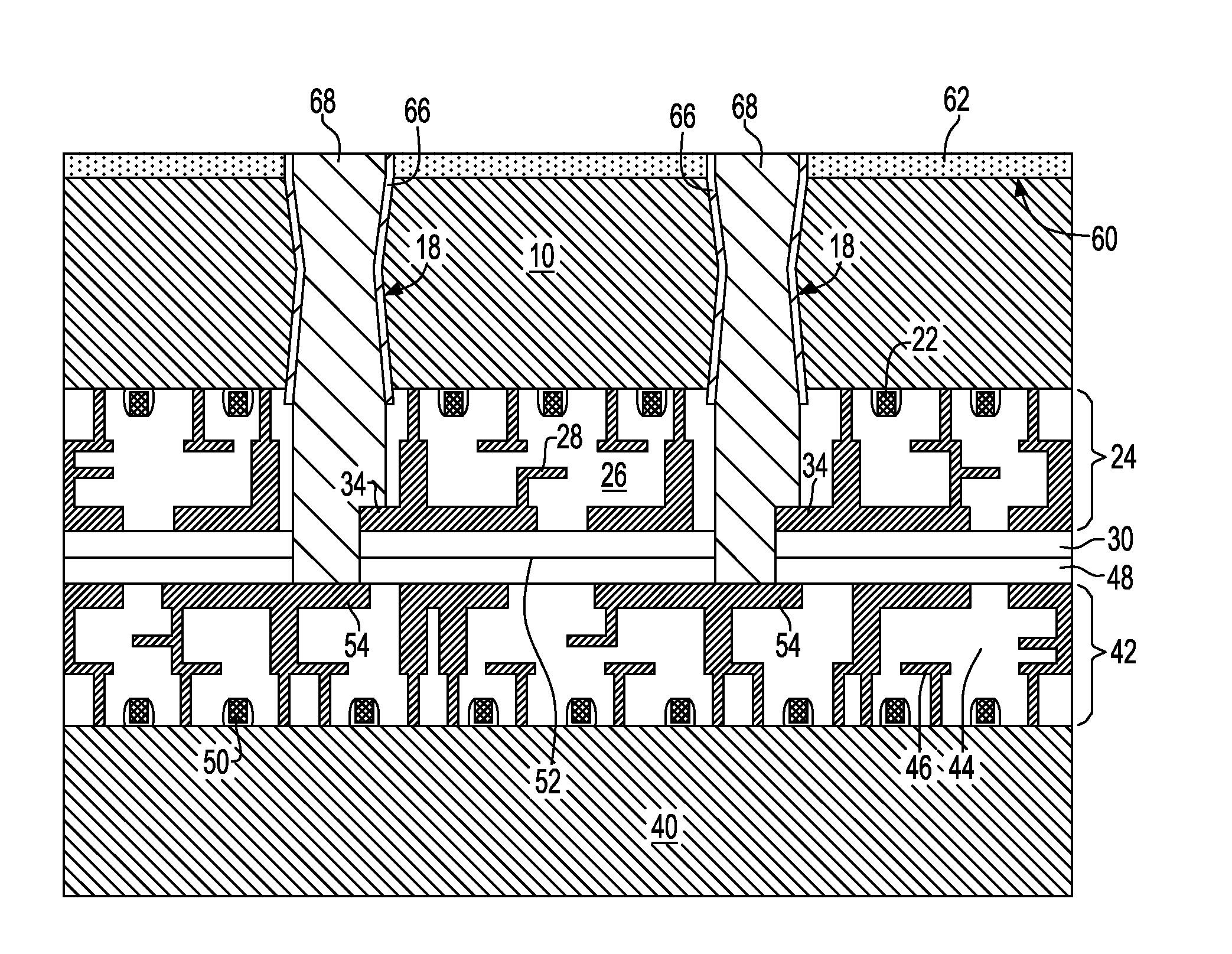
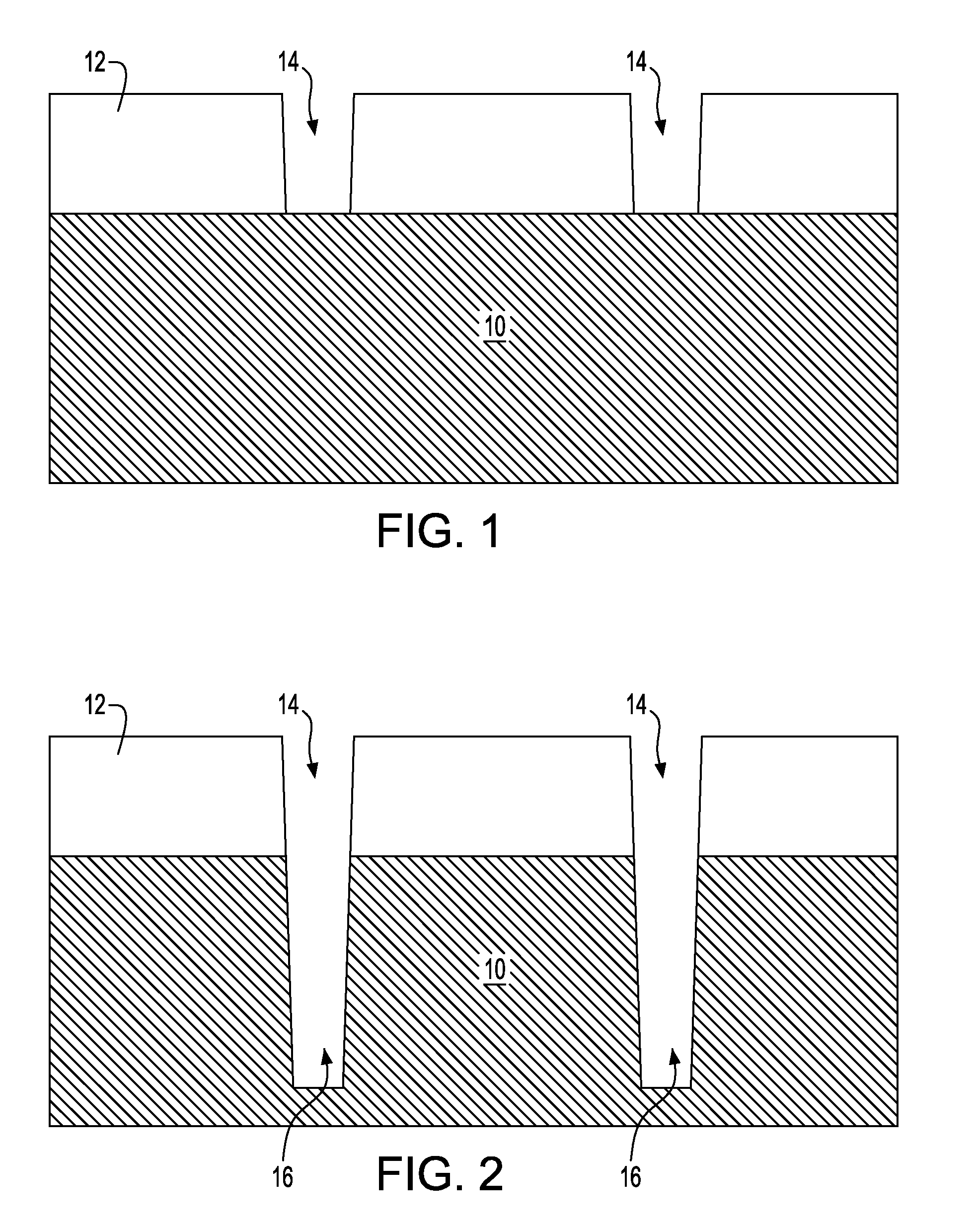
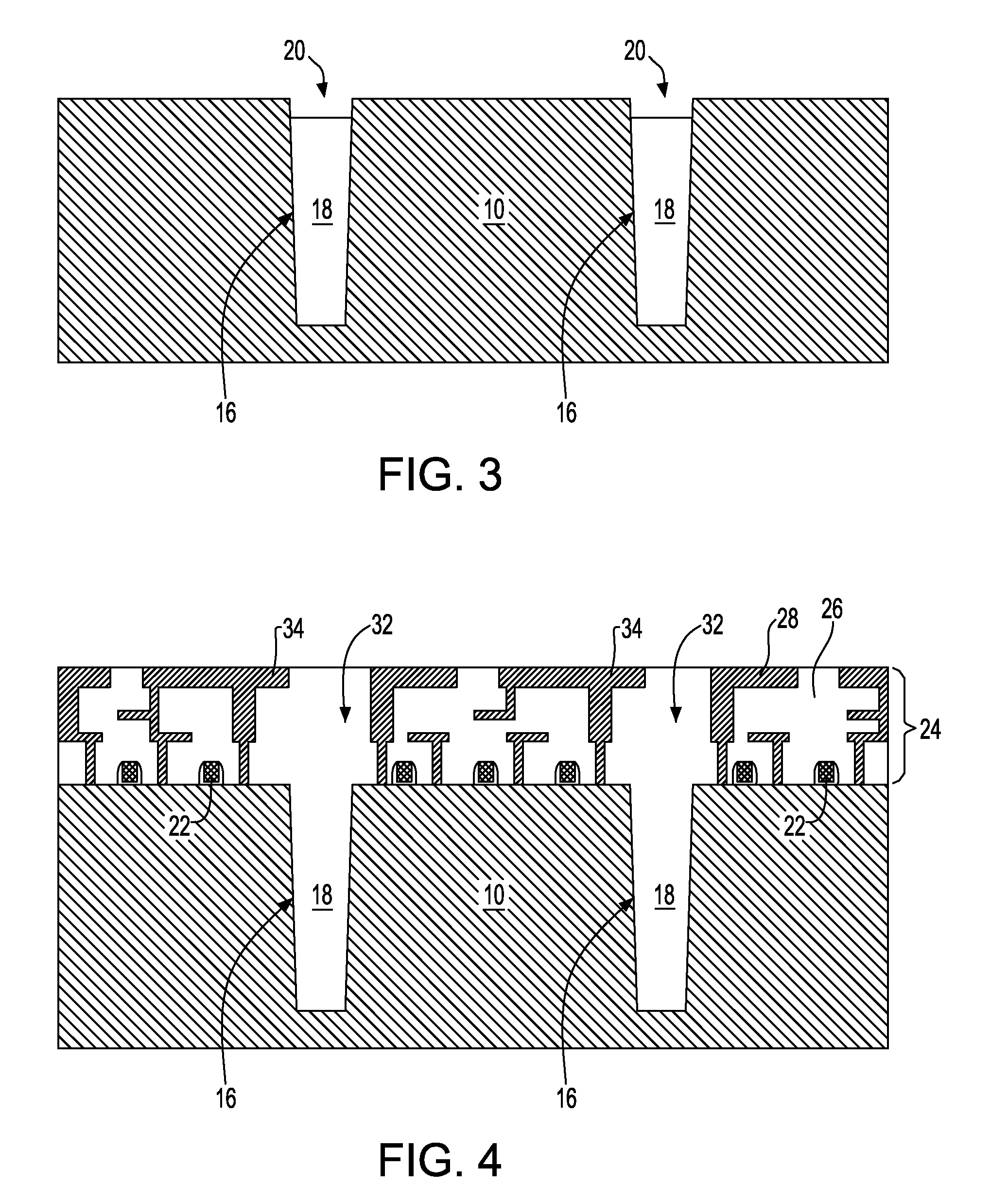
[0033]When semiconductor chips or integrated circuits (hereafter referred to as just “integrated circuits”) are joined to form a 3D structure, it is necessary to form vias through the semiconductor wafer to make the various connections between integrated circuits. These through silicon vias may be made on each integrated circuit before the integrated circuits are joined in a so-called through-silicon-first process. Alternatively, these through silicon vias may be made after the integrated circuits are joined in a so-called through-silicon-last process. The through-silicon-last process has an advantage of better connectivity over through-silicon-first but the through-silicon-last process also increases the difficulty in aligning through silicon vias to top and bottom semiconductor wafers simultaneously. The present invention relates to an improved process and structure for forming through silicon vias in a through-silicon-last process.

[0034]Referring now to the drawings in more detai...


PUM


Abstract

A method and structure of connecting at least two integrated circuits in a 3D arrangement by a through silicon via which simultaneously connects a connection pad in a first integrated circuit and a connection pad in a second integrated circuit.

Description

[0001]This non-provisional application claims the benefit of the provisional application filed with the United States Patent and Trademark Office as Ser. No. 61 / 149,529 entitled “A Method Of Making 3D Integrated Circuits And Structure Formed Thereby” filed Feb. 3, 2009.BACKGROUND OF THE INVENTION[0002]The present invention relates generally to three dimensional (3D) integrated circuits, and more particularly to 3D integrated circuits with through silicon vias.[0003]Since the invention of the integrated circuit, the semiconductor industry has experienced continual rapid growth due to continuous improvements in the integration density of various electronic components (i.e., transistors, diodes, resistors, capacitors, etc.). For the most part, this improvement in integration density has come from repeated reductions in minimum feature size, allowing for the integration of more components into a given area.[0004]These integration improvements are essentially two-dimensional (2D) in natu...

Claims


Application Information

Patent Timeline
Patent Type & Authority Patents(United States)
IPC IPC(8): H01L21/44
CPCH01L21/76898H01L23/481H01L25/0657H01L25/50H01L2224/80896H01L2224/83894H01L2225/06541H01L2224/9202H01L2224/80895H01L2224/81894H01L2224/9212H01L2224/8203H01L2224/821H01L2224/80001H01L2224/82
Inventor FAROOQ, MUKTA G.IYER, SUBRAMANIAN S.KOESTER, STEVEN J.ZHU, HUILONG
Owner GLOBALFOUNDRIES US INC
Why Eureka
Try Eureka