

Power supply circuit and semiconductor device for use therein
a power supply circuit and semiconductor technology, applied in the direction of electric variable regulation, process and machine control, instruments, etc., can solve the problems and achieve the effect of increasing chip size and cos
- Summary
- Abstract
- Description
- Claims
- Application Information
AI Technical Summary
Benefits of technology
Problems solved by technology
Method used
Image

Examples
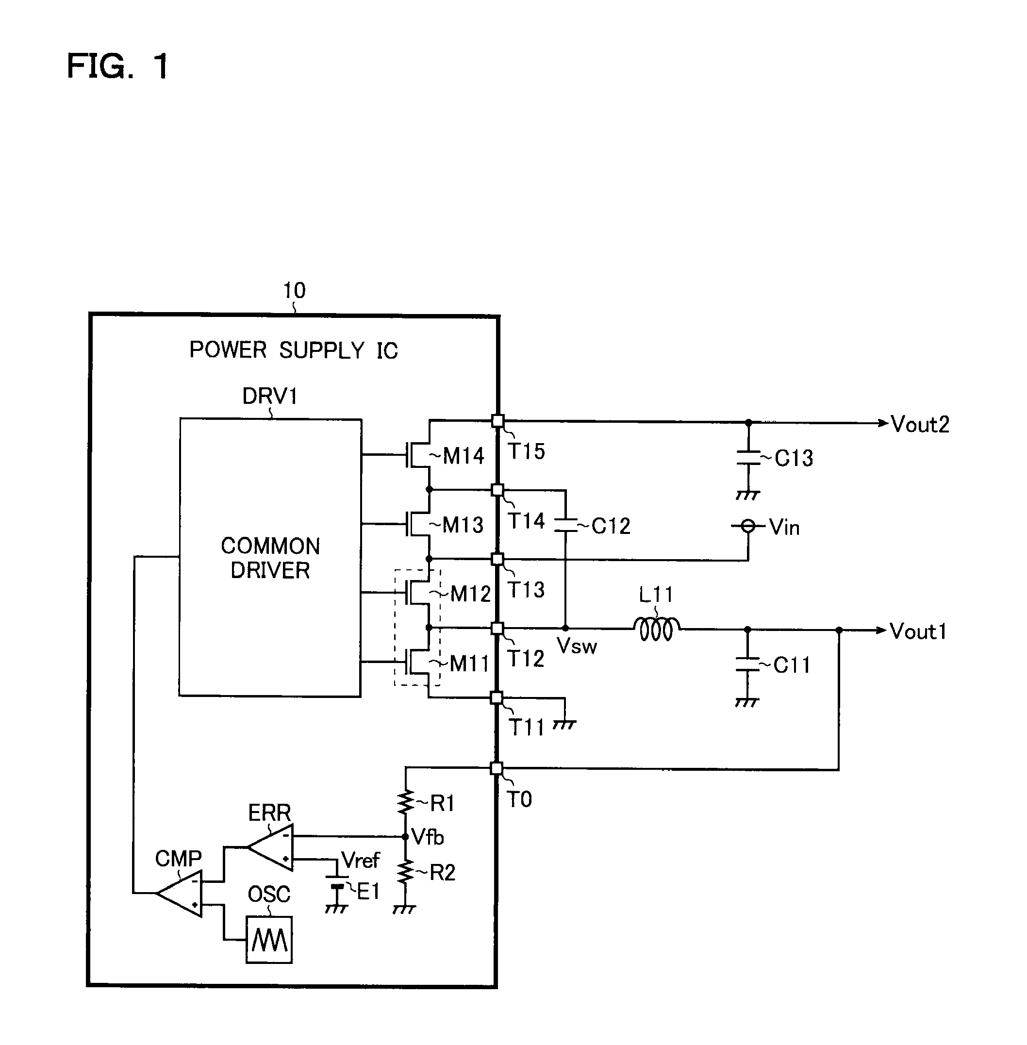
first embodiment
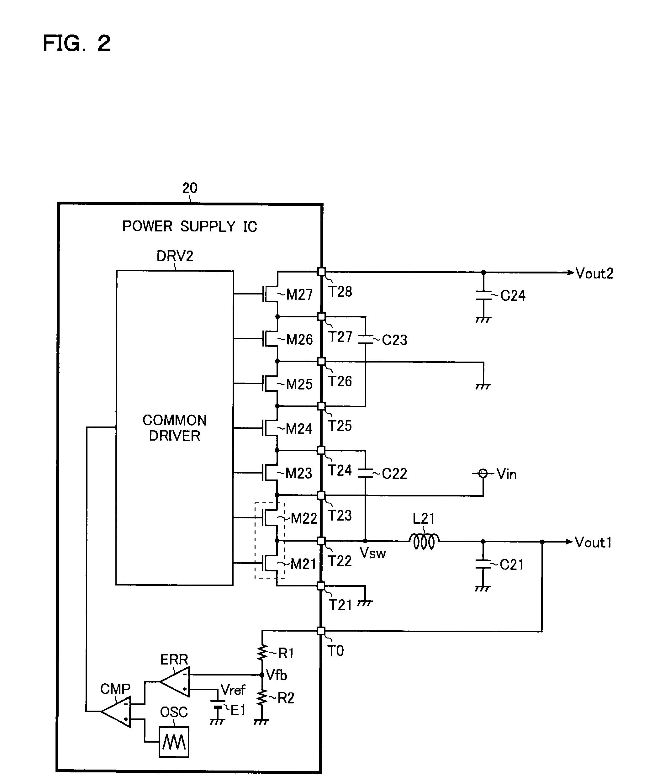
[0041]Inside the power supply IC 20, the transistor M 21 is connected between the terminals T21 and T22. The transistor M22 is connected between the terminals T22 and T23. The transistor M23 is connected between the terminals T23 and T24. The transistor M24 is connected between the terminals T24 and T25. The transistor M25 is connected between the terminals T25 and T26. The transistor M26 is connected between the terminals T26 and T27. The transistor M27 is connected between the terminals T27 and T28. Gates of the transistors M21 to M27 are each connected to the common driver DRV2. The connection relationship among the resistors R1 and R2, the error amplifier ERR, the DC voltage supply E1, the oscillation circuit OSC, the comparator CMP, and the common driver DRV2 is similar to that of the first embodiment described above, and thus no overlapping description thereof will be repeated.
[0042]Outside the power supply IC 20, the terminal T21 is connected to a ground terminal. The termina...
second embodiment
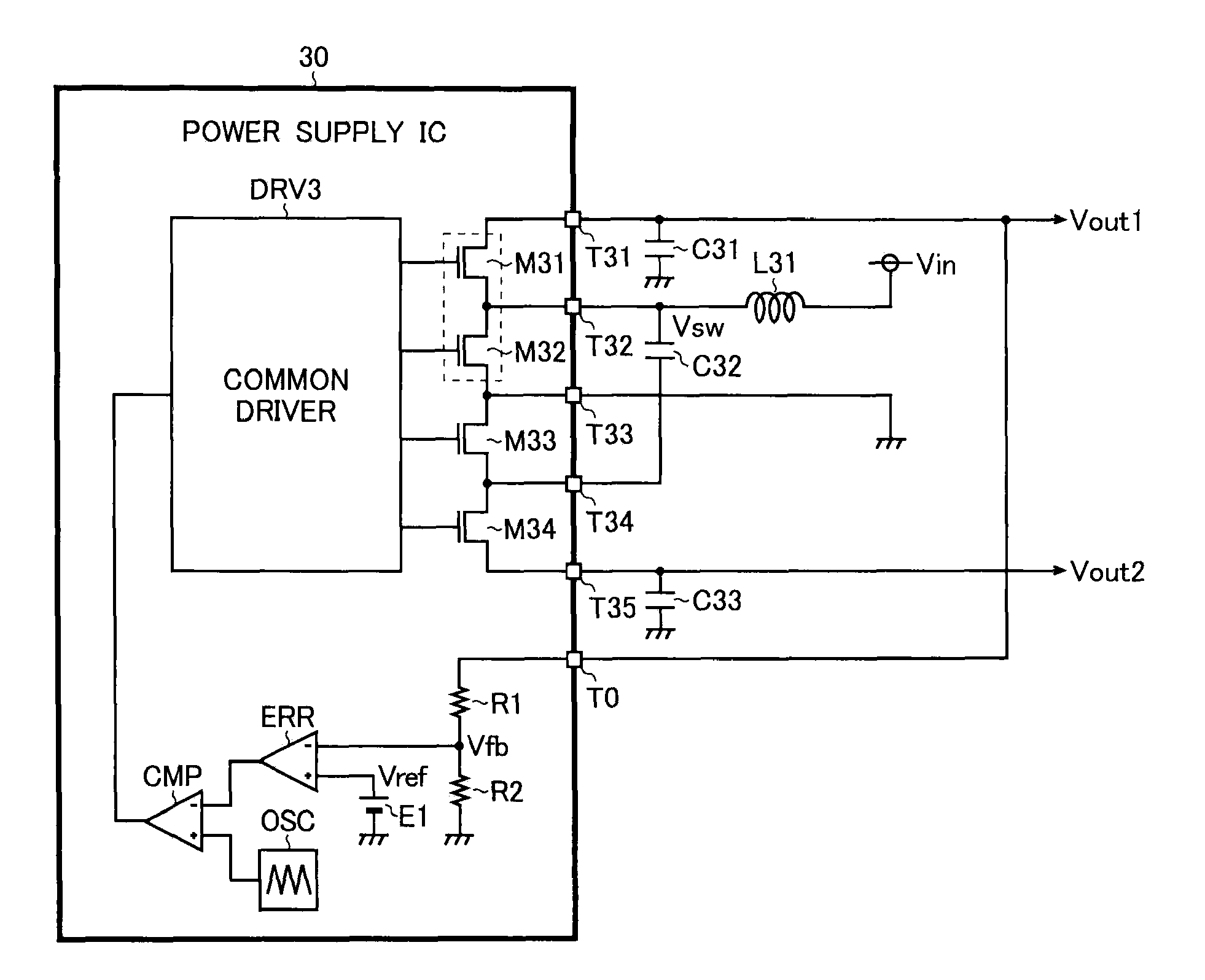
[0054]In the power supply IC 30, the transistor M31 is connected between the terminals T31 and T32. The transistor M32 is connected between the terminals T32 and T33. The transistor M33 is connected between the terminals T33 and T34. The transistor M34 is connected between the terminals T34 and T35. Gates of the transistors M31 to M34 are each connected to the common driver DRV3. The connection relationship among the resistors R1 and R2, the error amplifier ERR, the DC voltage supply E1, the oscillation circuit OSC, the comparator CMP, and the common driver DRV2 is similar to that of the first or second embodiment described above, and thus no overlapping description thereof will be repeated.
[0055]Outside the power supply IC 30, the terminal T31 is connected to a terminal from which an output voltage Vout1 is outputted, and is also connected to a first end of the capacitor C31. A second end of the capacitor C31 is connected to a ground terminal. The terminal T32 is connected to a fir...
PUM
 Abstract
Description
Claims
Application Information