Image display apparatus
a technology of image display and display device, which is applied in the direction of discharge tube/lamp details, discharge tube/lamp details, cathode ray tube/electron beam tube, etc., can solve problems such as discharge, achieve high-brightness display, increase the breakdown voltage between the anode electrode and the discharge tube, and effectively use the effect of light emitted
- Summary
- Abstract
- Description
- Claims
- Application Information
AI Technical Summary
Benefits of technology
Problems solved by technology
Method used
Image
Examples
first example
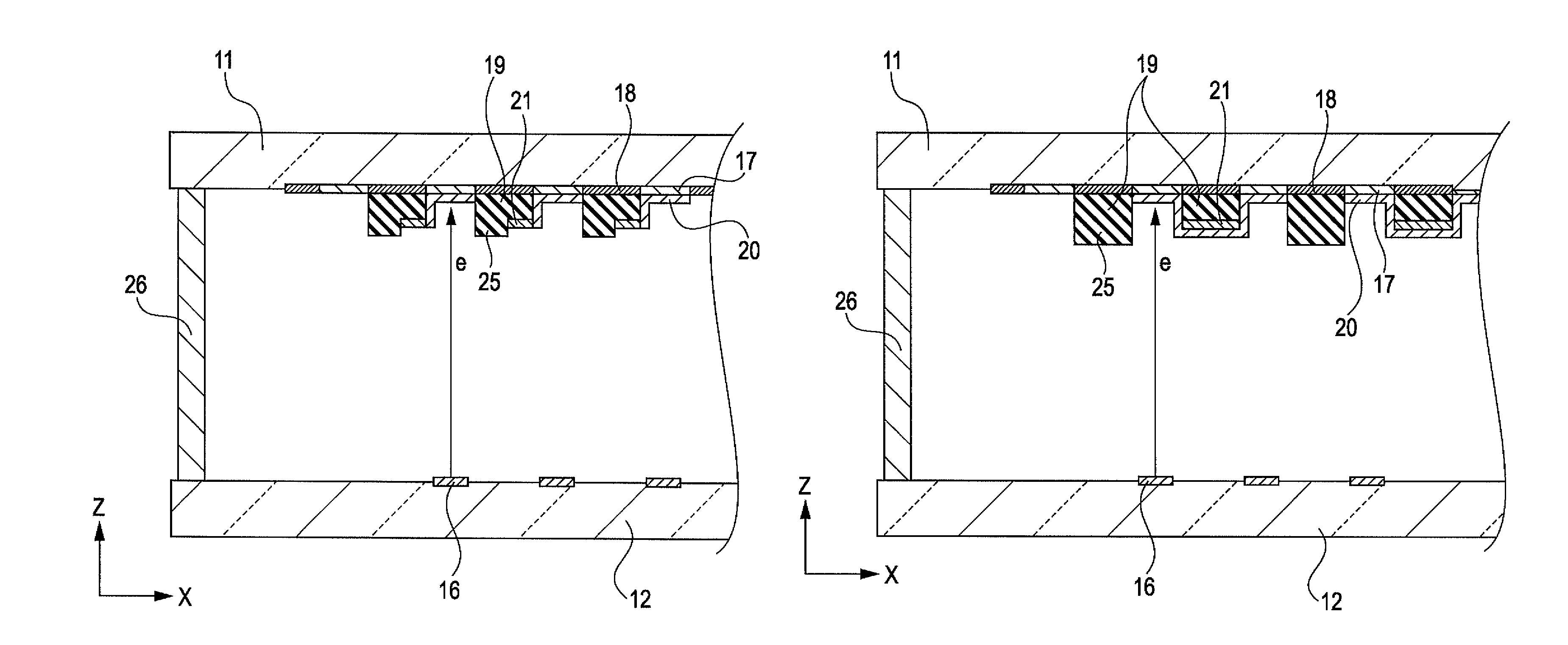
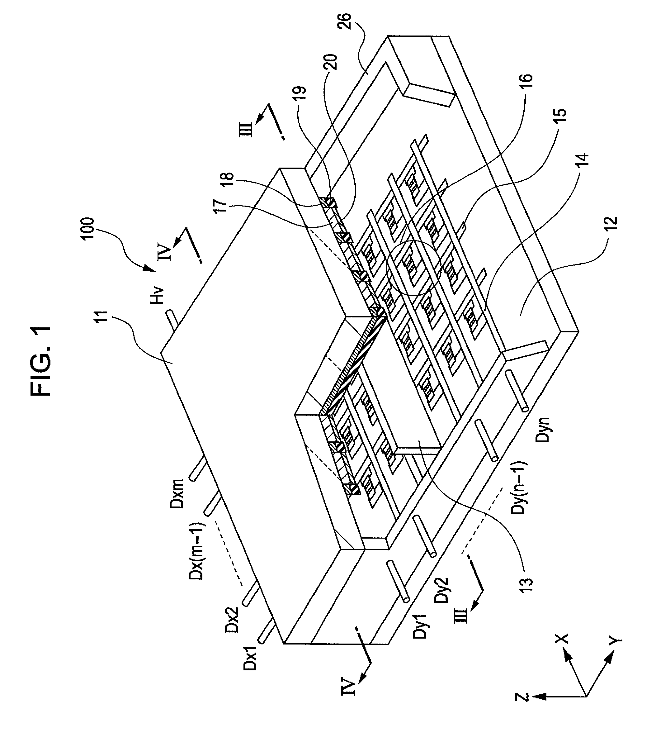
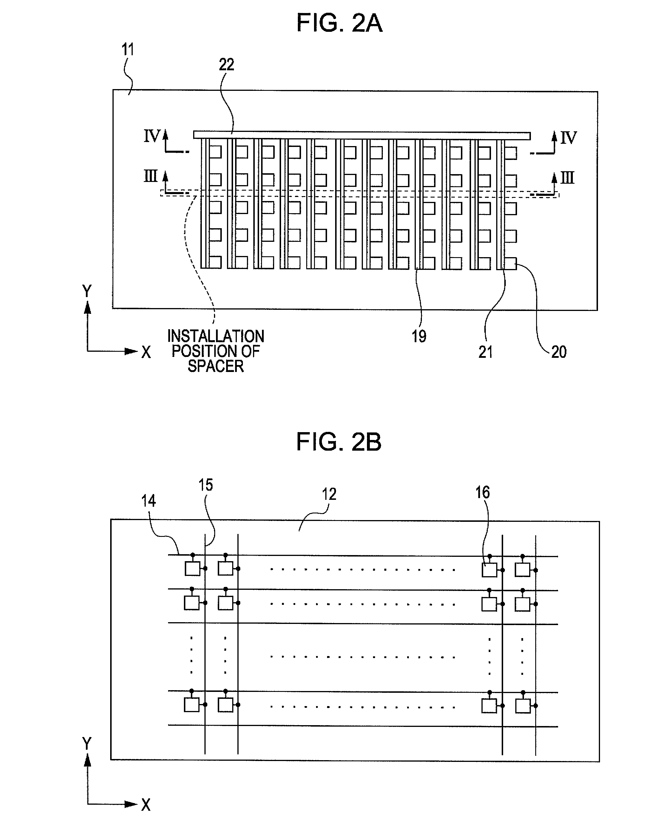
[0043]A first example of the present invention is described. Since the overall structure of the rear plate and the image display apparatus are described above, only the characteristics of the first example are described. FIG. 2A illustrates the face plate 11 of the first example viewed from the rear plate. FIGS. 3 and 4 are sectional views taken along lines III-III and IV-IV of FIG. 2A (or FIG. 1), respectively.
[0044]The face plate 11 of the first example was made as described below.
[0045](Step 1) A surface of a glass substrate was cleaned, strips of black paste (NP-7803D, made by Noritake Co., Ltd.) extending in the Y direction was screen printed on the surface with a width of 60 μm, and the glass substrate was dried at 120° C. and fired at 550° C., so that the light-shielding members 18 having a thickness of 5 μm was formed. The intervals (gaps) between the light-shielding members 18 in the X direction were 90 μm. The pitch of the light-shielding members 18 in the X direction was ...
second example
[0058]A second example of the present invention is described. The basic structure of the second example is the same as that of the first example. The first and second examples differ in that a face plate illustrated in FIGS. 8 and 9 was used in the second example.
[0059]Advantages similar to those of the first example were gained with the second example. The portions of the strip-shaped resistive members 21 at which strip-shaped resistive members 21 were connected to the anode electrodes 20 were covered with the anode electrodes 20. Thus, the anode electrodes 20 were electrically connected to the strip-shaped resistive members 21 more securely, so that the voltage of the anode electrodes becomes stable and a more excellent image was displayed.
third example
[0060]A third example of the present invention is described. The basic structure of the third example is the same as that of the first example. The first and third examples differ in that, in the third example, a face plate illustrated in FIGS. 5 to 7 was used and a conductive spacer was used as the spacer 13.
[0061]A method of making the face plate 11 used in the third example is described.
[0062]Steps 1, 2, and 4 of the first example were performed in the third example. Step 3 was not performed. Subsequent to step 4, the following steps 5-1 and 5-2 were performed.
[0063](Step 5-1) On the preforms of the partition members having been thus patterned, a high-resistant paste including ruthenium oxide was applied to alternate columns in the X direction in FIG. 5 (even number columns in FIG. 5) such that the paste had a layer thickness of 5 μm using a dispenser, and the preforms were dried for ten minutes at 120° C. The volume resistivity of the high resistance paste, which was measured by...
PUM
 Abstract
Description
Claims
Application Information


