
Automatic common-mode rejection calibration

a common-mode rejection and calibration technology, applied in the circuit field, can solve the problems of dc elimination, high common-mode rejection, and the possibility of amplifying differential signals, and achieve the effect of improving the balancing of the operation point and enhancing the cmrr

Active Publication Date: 2012-05-08
NXP BV
View PDF10 Cites 4 Cited by
  • Summary
  • Abstract
  • Description
  • Claims
  • Application Information

AI Technical Summary

Benefits of technology

This approach effectively reduces power consumption, speeds up processing, and improves common-mode rejection by efficiently managing DC offsets and noise, enabling faster and more accurate biopotential signal acquisition with reduced memory requirements.

Problems solved by technology

There are two major issues in the design of front-ends for these systems: firstly, dealing with a differential DC offset superimposed on a much smaller useful signal and secondly, obtaining a high common-mode rejection.
The DC offset or DC component, respectively, in the differential signal introduces two major problems.
Firstly, if only a low supply is available, it is not possible to amplify the differential signal before the DC is eliminated.
Secondly, the presence of a high DC component brings an unbalance in the operation point of any circuit in the signal path.
As it will be clarified in the following, this unbalance degrades the common-mode rejection.
This unbalance cannot be eliminated by the usual techniques used to improve the common-mode rejection ratio (CMRR), as chopping.
The reason is, that the unbalance is embedded in the differential signal and it would be chopped with it.
If very particular techniques are not used, the very low frequency singularities of the filter bring problems of integrability.
Another disadvantage of the filter solution is a very slow startup and slow response to abrupt variations of Vdm,DC caused for example by motional artifacts.
This can be an excessive overhead if the system is used for sensing the heartbeats for only a few minutes.
However, such circuitry is not optimized in terms of power, since the DC offset is treated as useful signal, increasing the required resolution and the power consumption.

Method used


Image

  • Automatic common-mode rejection calibration
  • Automatic common-mode rejection calibration
  • Automatic common-mode rejection calibration

Examples


first embodiment

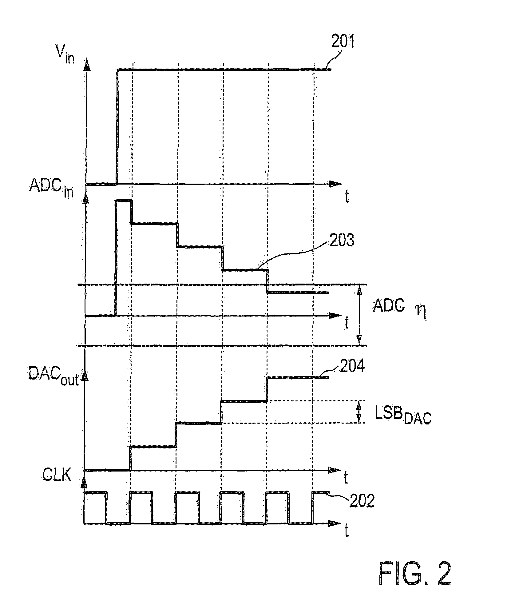
[0042]In a first embodiment, the calibration signal is stored as calibration sequence q whose actual values define in which of the at least two unbalanced states the system is put in any particular instant. In a basic implementation, the calibration sequence q is a binary sequence comprised of two kinds of symbols each being associated with one of two different unbalanced states. It is noted that the calibration signal that determines the unbalanced state of the system can be designed to have a rate or frequency, respectively, much higher than the characteristic frequency of the system. If the introduced unbalances and the calibration sequence q are chosen in an appropriate way, the time average of the differential output results in a compensation of the introduced unbalances by means of the averaging. Methods to choose and to generate the right unbalance and the calibration sequence q are described in the following.

[0043]Preferably, the compensation is performed in the first block ...

third embodiment

[0088]FIG. 8 illustrates simulation results of different methods for generating the calibration sequence q according to the present invention. The simulations have been repeated in three cases: with an ideal transconductor (see solid line in FIG. 8), i.e. gmd independent from q (gmd=gmd0)); with a transconductor with gmd variations of ±1% dependent on the value of q (gmd=gmd0(1+k q)) when using the system for ILA depicted in FIG. 7 (see dotted line in FIG. 8); with a transconductor with gmd variations of ±1% dependent on the sequence q and using a calibration sequence qs obtained from a single digital modulator, i.e. no ILA (see dashed line in FIG. 8). The common-mode tone is buried under noise level: in this case the average q used was ideal and the use of a pseudo-random sequence results in a very high CMRR. The folding of quantization noise can be clearly seen for the case when ILA is not adopted (see dashed line in FIG. 8). With ILA (see dotted line in FIG. 8) no folding is pres...


PUM


Abstract

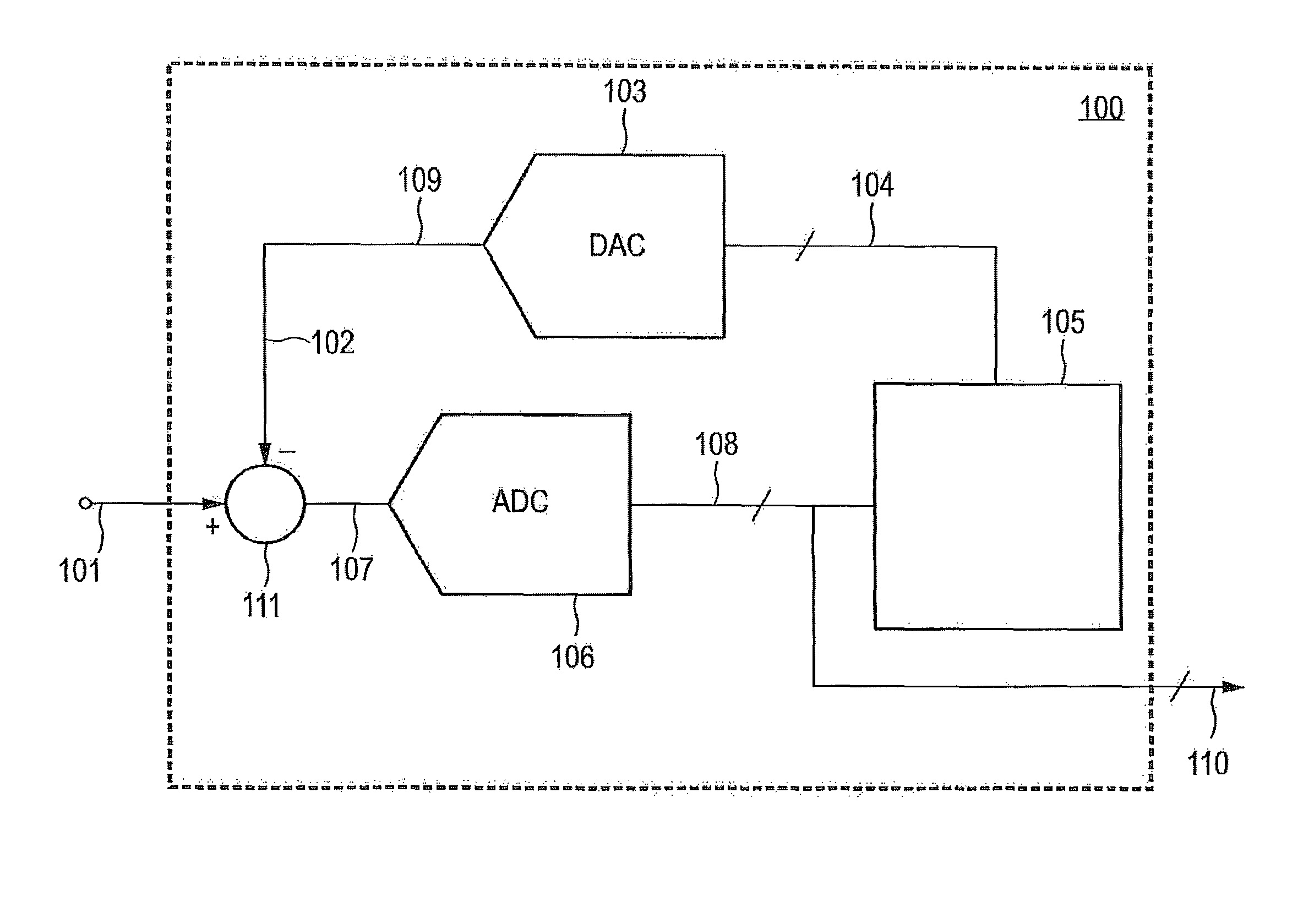
The present invention relates to a circuit and a method for automatic common-mode rejection calibration in a differential conversion system and unbalance compensation for balancing the operation point of a circuit in the signal path and for enhancing the common-mode rejection. The circuit for automatic common-mode rejection calibration in a differential conversion system comprises an analog input stage for an analog input signal (101), an analog-digital-converter (106) for converting an analog signal (107) into its digital representation (108), a digital block (105) arranged to adapt said digital representation (108) of a portion of a DC offset of said analog input signal (101) in accordance with whether said analog input signal (101) is in a predetermined input range of said analog-digital-converter (106), and a digital-analog-converter (103) arranged in a feedback path (102) from said digital block (105) to subtraction means (111) of said analog input stage for converting a digital signal (104) into an analog output signal (109), wherein said analog output signal (109) is subtracted from said analog input signal (101) resulting in said analog signal (107).

Description

FIELD OF THE INVENTION[0001]The present invention relates to a circuit and a method for automatic common-mode rejection calibration and unbalance compensation, e.g. for balancing the operation point of a circuit in a signal path and enhancing the common-mode rejection.BACKGROUND OF THE INVENTION[0002]Biopotential reading systems are used to electronically acquire electric signals from human body, such as heart signals as an electrocardiogram (ECG) and brain activity as an electroencephalogram (EEG). These systems can be used in any biopotential acquisition system, not only as ECG or EEG, but also in electromyography (EMG). They are also needed in different applications, including Body Area Networks (BANs). However, to be embedded in sensor nodes for such a power constrained application as for BANs, special techniques should be employed to meet special requirements such as relating to the power.[0003]An ECG illustrates the electrical activity of the heart over time. Analysis of the v...

Claims


Application Information

Patent Timeline
Patent Type & Authority Patents(United States)
IPC IPC(8): H03M1/06H03M3/00
CPCH03F1/304H03F3/4565H03F2203/45504H03F2203/45456H03F2203/45471H03F2203/45448
Inventor SEBASTIANO, FABIOBREEMS, LUCIEN JOHANNESROOVERS, RAF LODEWIJK JAN
Owner NXP BV
Learn More