Sensor device having non-contact charge function and containers having the same
a sensor and non-contact technology, applied in the direction of independent non-interacting antenna combinations, differential interacting antenna combinations, instruments, etc., can solve the problems of high charge sensitive of the antenna, the ic tag of the sensor, the mounting of the sensor, etc., and achieve significant antenna gain and improve the charge function
- Summary
- Abstract
- Description
- Claims
- Application Information
AI Technical Summary
Benefits of technology
Problems solved by technology
Method used
Image
Examples
embodiment mode 1
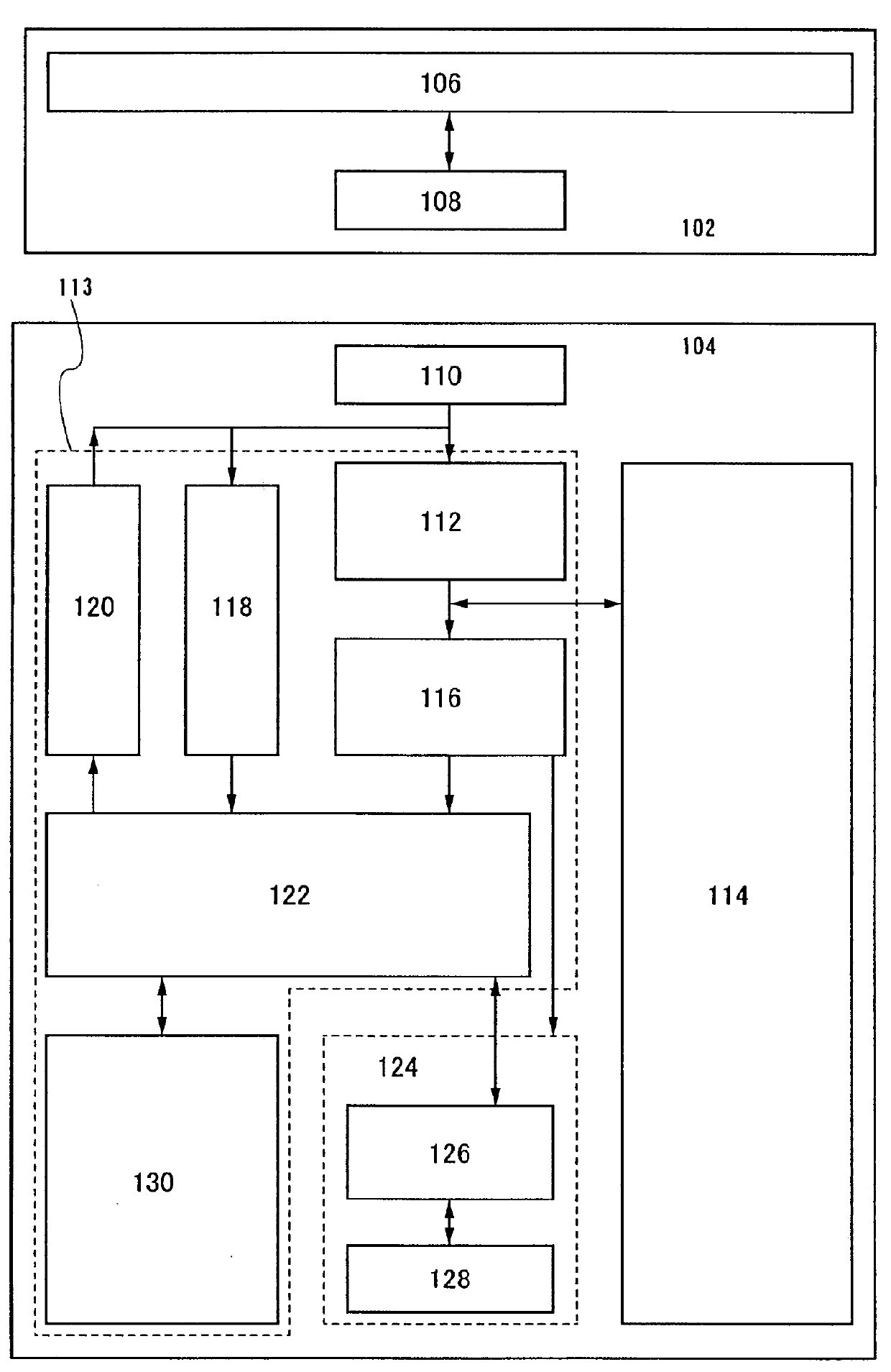
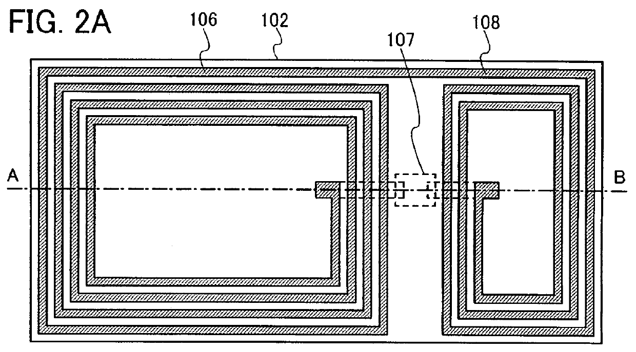
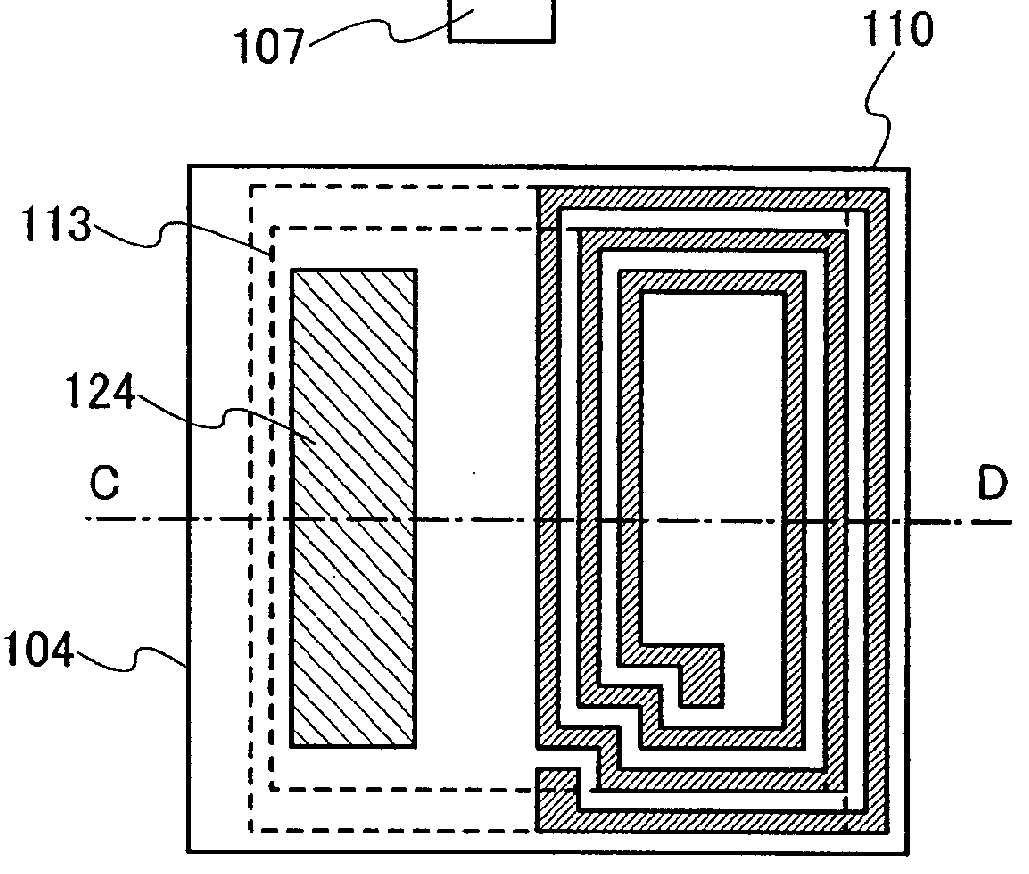
[0037]This embodiment mode will describe a structure in which an antenna for receiving electromagnetic waves and a sensor portion are provided on different bases in order to miniaturize the sensor device having a non-contact charge function with reference to drawings. In addition, this embodiment mode will describe a structure of the sensor device in which a first antenna for receiving electromagnetic waves is formed over a first base, and a CPU, a sensor portion, and a power storage portion for supplying electric power thereto are provided over a second base.
[0038]FIG. 1 is a block diagram showing a structure of the sensor device in accordance with this embodiment mode. This sensor device is composed of a first base 102 and a second base 104, which is separated from the first base 102. A first antenna 106 receiving electromagnetic waves is provided to the first base 102. The first antenna 106 constantly receives electromagnetic waves of from a submillimeter-wave band to a very long...
embodiment mode 2
[0055]This embodiment mode will describe another structure in which an antenna receiving electromagnetic waves and a sensor portion are provided with different bases so that a sensor device having a non-contact charge function can be miniaturized as in Embodiment Mode 1. In this embodiment mode, the sensor device, in which a first antenna receiving electromagnetic waves, a CPU, and a power storage portion are formed over a first base, and a sensor portion is provided over a second base, will be described.
[0056]FIG. 4 is a block diagram showing a structure of the sensor device in accordance with this embodiment mode. This sensor device is composed of a first base 102 and a second base 104. The first base 102 and the second base 104 are separate bases. The first base 102 has a power storage portion 114 and a circuit portion 144 of the first base. The second base 104 has a circuit portion 146 of the second base and a sensor portion 124.
[0057]A first antenna 131 receiving electromagneti...
embodiment mode 3
[0068]This embodiment mode will describe an example of a first base 102 that has a different mode from Embodiment Mode 2 with reference to FIG. 7 and FIG. 8. This embodiment mode shows an example of a sensor device having plural antennas to receive wide bands of electromagnetic waves and store electric power.
[0069]In a first base 102 described in FIG. 7, a circuit portion 144 of the first base includes components such as a rectification circuit 112, a constant-voltage circuit 116, an oscillation circuit 117, a demodulation circuit 118, a modulation circuit 120, a CPU 122, and a memory portion 130. A structure of the circuit portion 144 has functions similar to those in FIG. 4.
[0070]A first antenna 131 is used for transmission / reception of control commands or communication data, to / from an external device. A demodulation circuit 148 and a modulation circuit 150, which are connected to the first antenna 131 are circuits performing modulation / demodulation of control demands or communic...
PUM
 Abstract
Description
Claims
Application Information


