Digital readout method and apparatus

a digital readout and digital technology, applied in analogue/digital conversion, television systems, instruments, etc., can solve the problems of limiting the practical scalability of conventional designs, specific analog designs can target (and possibly achieve) one or more requirements, and fail, etc., to achieve the elimination of highly linear analog electronics, and the effect of large charge storage capacitors

Active Publication Date: 2012-05-15
MASSACHUSETTS INST OF TECH
View PDF39 Cites 99 Cited by
  • Summary
  • Abstract
  • Description
  • Claims
  • Application Information

AI Technical Summary

Benefits of technology

[0011]In an illustrative embodiment an all-digital readout integrated circuit (ROIC) in accordance with the principles of the present invention may be used in conjunction with a cryogenically cooled infrared detector array, with connections between the detector array and the ROIC made via indium bump bonding. The hybrid device thus formed is referred to herein as a digital focal plane array (DFPA). In an illustrative embodiment, the detector array senses incoming optical radiation in the infrared region of the spectrum (2-20 microns) using photodiodes to create currents that are proportional to the optical radiation impinging on the photodiodes. That is, each photodiode (also referred to herein as a pixel) in the detector array produces a current that is proportional to the photon flux impinging upon it. Each photodiode in the array has associated with it a unit cell in the ROIC. The current in each photodiode is collected in the photodiode's associated unit cell within the ROIC. The unit cell electronics integrate the charge and produces, via an analog to digital converter (ADC), a digital number (DN) that is proportional to the total charge accumulated over the frame period. In this illustrative embodiment, the DN for each pixel is then shifted to the edge of the ROIC and multiplexed with other DNs associated with other pixels for transfer off the array. By digitizing the signal while photoelectrons are being collected, rather than after charge accumulation, the need for large charge storage capacitors and highly linear analog electronics can be eliminated. The power dissipation and noise problems associated with a conventional, analog readout, approach are also greatly reduced. Additionally, this approach permits operation with circuitry that operates from a lower level power supply, because the dynamic range requirements associated with conventional systems needn't be maintained. Permitting operation with lower-level power supplies permits the use of Integrated Circuit processes that offer much smaller feature sizes, thereby further enabling the ADC and readout circuitry to be packed within an area less than or equal to the area consumed by the associated detector pitch, also referred to as the pixel pitch. Simplifying the unit cell preamplifier offers considerable power savings for large arrays.
[0012]In this illustrative embodiment, the capacitor size defines the least significant bit of the ADC. In this way, the size of the capacitor may be kept to a minimum, thereby significantly reducing the area required for the analog to digital conversion. In this illustrative embodiment, the analog to digital conversion is achieved via a voltage-to-frequency converter in which a predetermined amount of photocurrent charges the capacitor to a level that produces an output pulse and resets the capacitor. The output pulses are counted and the count in a given time period corresponds to the amount of photocurrent and, correspondingly, the light flux impinging on the associated photodiode. In this way, the illustrative embodiment of a DFPA in accordance with the principles of the present invention digitizes the signal while photoelectrons are being collected, rather than after charge accumulation.
[0016]An apparatus and method in accordance with the principles of the present invention may also be employed by a DFPA to incorporate on-chip processing to further enhance the DFPA's performance. Such processing may include: digital spatial / temporal filtering that may be implemented by pixel binning whereby image resolution may be traded for dynamic range and / or frame rate; autonomous digital threshold detection that may be used in launch detection or flash detection, for example; time domain digital filtering, such as high-pass or low-pass filtering that may be employed to identify fast- or slow-moving objects; time domain image detection and jitter compensation that, for example, that shifts digital row data synchronously with ground speed and provides image stabilization for field of view jitter; data compression to reduce raw data rate using, for example, decimation; and the use of edge enhancement, such as octonet edge enhancement to aid in feature identification.

Problems solved by technology

Conventional FPAs are not particularly well-suited to satisfying combinations of the above requirements.
Specific analog designs can target (and possibly achieve) one or more requirement, but fail when simultaneously targeting the most aggressive design parameters for imaging applications, such as long-wave infrared imaging (LWIR) applications.
Fundamental limitations on achievable well depth (with concomitant limitations on capacitor size), and the readout noise floor, limit practical scalability of conventional designs.
Capacitor size limitations require unnecessarily high frame rates to avoid saturating pixels.
Attempting to scale conventional analog technology to meet the most demanding requirements leads to a high-power-consumption FPA with many data output taps.
This in turn leads to a large, massive, and complex sensor system.

Method used


Image

  • Digital readout method and apparatus
  • Digital readout method and apparatus
  • Digital readout method and apparatus

Examples


Embodiment Construction

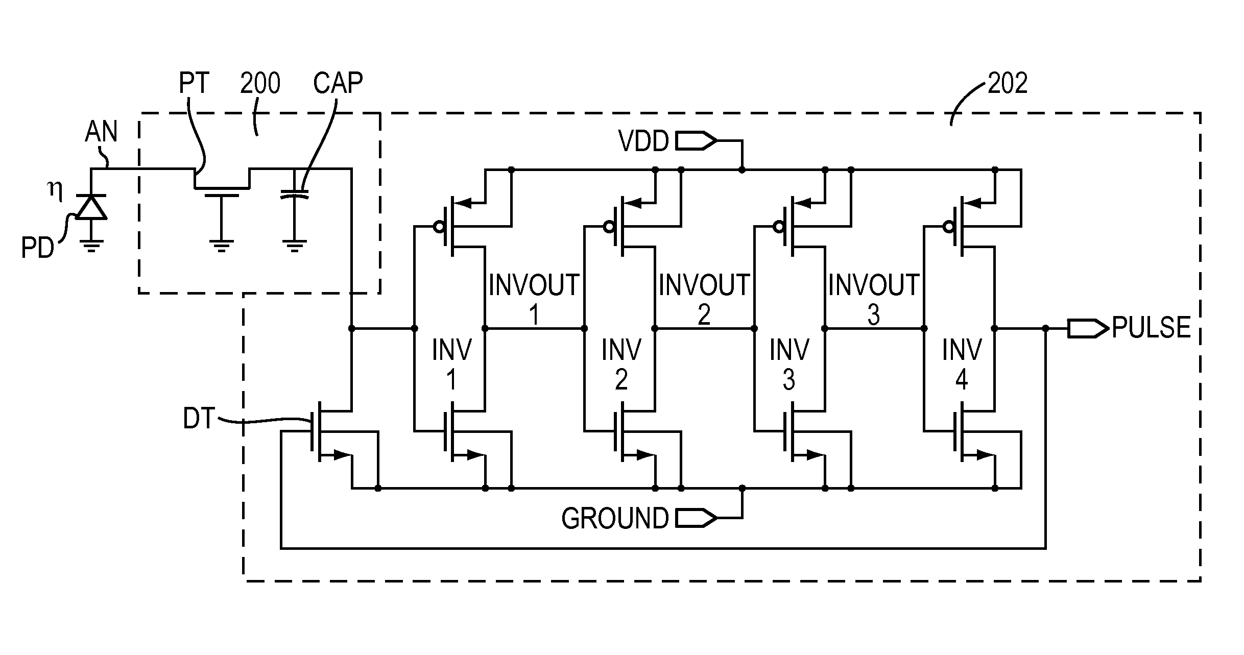
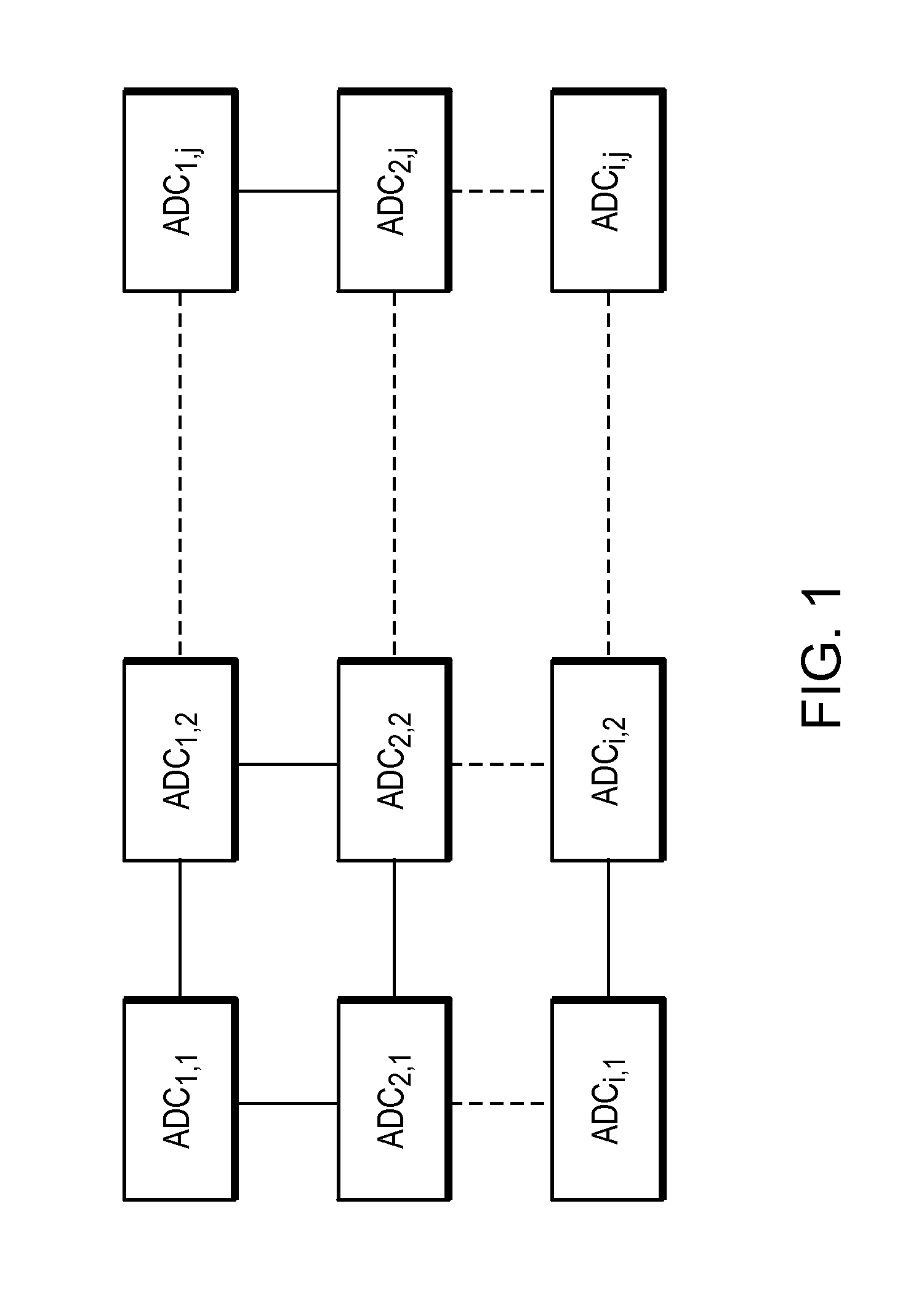
[0030]The block diagram of FIG. 1 illustrates an apparatus in accordance with the principles of the present invention that includes a two-dimensional array 100 of analog to digital converters (ADCs), ADCi,j (where i=1 through n and j=1 through m). In this illustrative embodiment, the ADCs are all self-contained. That is, in such an embodiment, each of the ADCs is capable of operating without signaling, such as an analog ramp signal, or analog reference signal supplied by an outside source. Each of the ADCs within the array may include circuitry to convert a current mode signal to a voltage signal for conversion. In such an embodiment, a capacitor may be employed to integrate charge from the current mode signal and the capacitor and ADC architecture may be selected to determine the least significant bit of each of the ADCs. In such an embodiment, a counter may be employed to determine the most significant bit of each of the ADCs.

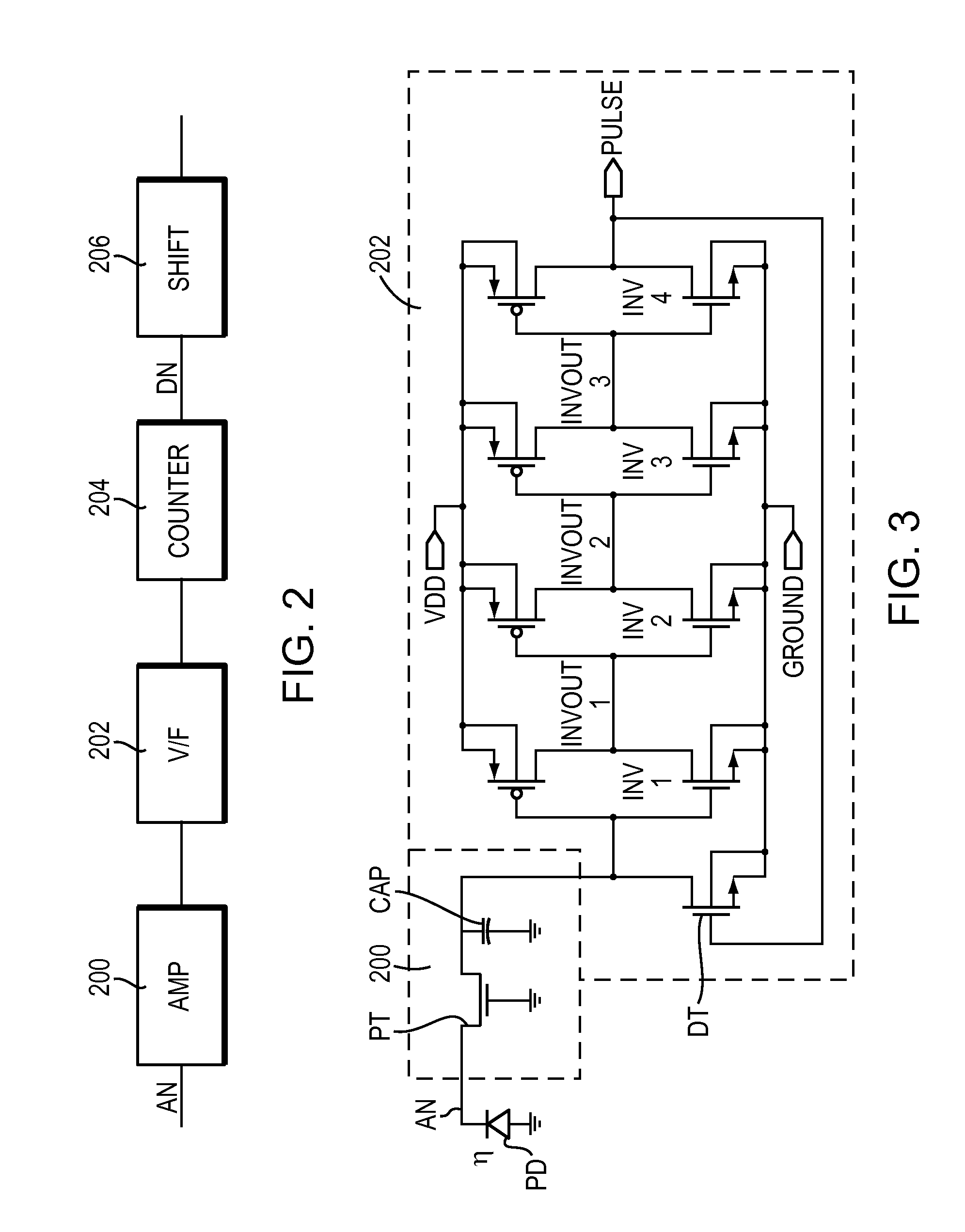
[0031]The block diagram of FIG. 2 provides a more detai...


PUM


Abstract

Autonomously operating analog to digital converters are formed into a two dimensional array. The array may incorporate digital signal processing functionality. Such an array is particularly well-suited for operation as a readout integrated circuit and, in combination with a sensor array, forms a digital focal plane array.

Description

RELATED APPLICATIONS[0001]We claim benefit of Provisional Patent Application entitled, AN ALL DIGITAL READOUT INTEGRATED CIRCUIT ARCHITECTURE FOR VERY LARGE, HIGH FRAME RATE, AND WIDE DYNAMIC RANGE INFRARED IMAGING ARRAYS, filed on Sep. 30, 2005, and having inventors Michael Kelly, Daniel Mooney, Curtis Colonero, Robert Berger, and Lawrence Candell, and Ser. No. 60 / 722,741, which is hereby incorporated by reference in its entirety.GOVERNMENT SPONSORSHIP[0002]This work was made with government support under contract no. F19628-00-C-0002 awarded by the U.S. Air Force. The Government has certain rights in this invention.FIELD OF THE INVENTION[0003]The invention relates to analog to digital converters (ADCs) and, in particular, to collections of ADCs.BACKGROUND OF THE INVENTION[0004]ADCs are employed in a variety of applications. In particular, high performance focal plane array (FPA) applications require wide-area coverage, high signal-to-noise-ratios (SNR), high spatial resolution, an...

Claims


Application Information

Patent Timeline
Patent Type & Authority Patents(United States)
IPC IPC(8): H03M1/12
CPCH03M1/145H04N5/37455H04N5/3355H03M1/60H04N25/772H04N25/75H03M1/12
Inventor KELLY, MICHAELMOONEY, DANIELCOLONERO, CURTISBERGER, ROBERTCANDELL, LAWRENCE
Owner MASSACHUSETTS INST OF TECH
Why Eureka
Try Eureka