GaN crystal producing method, GaN crystal, GaN crystal substrate, semiconductor device and GaN crystal producing apparatus
a crystal substrate and gan crystal technology, applied in the direction of crystal growth process, conductive materials, non-conductive materials with dispersed conductive materials, etc., can solve the problem of not being able to fabricate an led on the non-polar surface of a gan crystal substrate, unable not being able to achieve high luminance, etc. problem, to achieve the effect of preventing nucleation, high-quality non-polar surface, and high crystallinity quality quality quality quality quality quality quality quality
- Summary
- Abstract
- Description
- Claims
- Application Information
AI Technical Summary
Benefits of technology
Problems solved by technology
Method used
Image

Examples
example 1
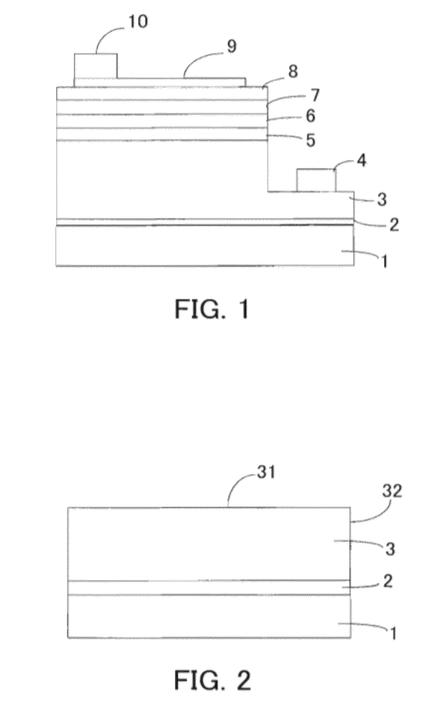
[0078]A GaN crystal was produced using the apparatus of FIG. 11. Specifically, a sapphire substrate on which a thin GaN film layer (its upper surface being a c-plane) was provided was initially placed in an alumina crucible 15. Sodium (Na), gallium (Ga) and carbon (C: graphite) also were placed in the alumina crucible 15. The molar ratio of sodium (Na) to gallium (Ga) was Na:Ga=73:27. The proportion of added carbon (C) to the total (Na+Ga+C) of sodium (Na), gallium (Ga) and carbon (C) was 0, 0.02, 0.1, 0.5, 1, 2, and 5 atoms % (at. %). Note that the case where the carbon proportion was 0 at. % is Comparative Example 1. The crucible 15 was placed in a stainless steel container 13. The stainless steel container 13 was placed in a heat- and pressure-resistant container 14. While nitrogen gas was introduced from the gas tank 11 to the stainless steel container 13, the heat- and pressure-resistant container 14 was heated using a heater (not shown) so that the inside thereof was at a high...
example 2
[0081]GaN crystals were produced in the same manner as that of Example 1, except that the reaction conditions for crystal growth were a temperature of 800° C. and a pressure of 50 atm (about 5.0 MPa), and the proportions of added carbon were 0 at. % (Comparative Examples 2 and 3), 1 at. %, 2 at. %, and 3 at. %. The results are shown in the graph of FIG. 9. In FIG. 9, open bars indicate the yields of GaN crystals that grew on the thin GaN crystal film layers (LPE yields), and closed bars indicate the yields of GaN crystals that grew in the melt after nucleation (nucleation yields). In FIG. 9, “no addition 1” corresponds to Comparative Example 2, and “no addition 2” corresponds to Comparative Example 3. As shown in the graph of FIG. 9, when carbon was not added, nucleation occurred, which blocked growth of a GaN crystal on the thin GaN crystal film layer. When carbon was added, nucleation was prevented, so that a GaN crystal having a high-quality non-polar surface grew on the thin GaN...
example 3
[0082]GaN crystals were produced in the same manner as that of Example 1, except that the reaction conditions for crystal growth were a temperature of 750° C. and a pressure of 50 atm (about 5.0 MPa), and the proportions of added carbon were 0 at. % (Comparative Examples 4, 5 and 6), 1 at. %, 2 at. %, and 3 at. %. The results are shown in the graph of FIG. 10. In FIG. 10, open bars indicate the yields of GaN crystals that grew on the thin GaN crystal film layers (LPE yields), and closed bars indicate the yields of GaN crystals that grew in the melt after nucleation (nucleation yields). In FIG. 10, “no addition 1” corresponds to Comparative Example 4, “no addition 2” corresponds to Comparative Example 5, and “no addition 3” corresponds to Comparative Example 6. As shown in the graph of FIG. 10, when carbon was not added, nucleation occurred, which blocked growth of a GaN crystal on the thin GaN crystal film layer. When carbon was added, nucleation was prevented, so that a GaN crystal...
PUM
| Property | Measurement | Unit |
|---|---|---|
| temperature | aaaaa | aaaaa |
| pressure | aaaaa | aaaaa |
| temperature | aaaaa | aaaaa |
Abstract
Description
Claims
Application Information
 - R&D Engineer
- R&D Manager
- IP Professional
- Industry Leading Data Capabilities
- Powerful AI technology
- Patent DNA Extraction
Browse by: Latest US Patents, China's latest patents, Technical Efficacy Thesaurus, Application Domain, Technology Topic.
© 2024 PatSnap. All rights reserved.Legal|Privacy policy|Modern Slavery Act Transparency Statement|Sitemap