Laminated body and manufacturing method thereof

a technology of laminated body and manufacturing method, which is applied in the direction of resistor details, resistor housing/enclosement/embedding, resistors adapted for applying terminals, etc., can solve the problems of inapplicability, lack of reliability of the same, and limited high density integration, so as to improve the connectivity of internal resistive elements and exterior electrodes, and the resistance variation of internal-layer resistive elements small

Active Publication Date: 2012-06-05
KOA CORP
View PDF14 Cites 4 Cited by
  • Summary
  • Abstract
  • Description
  • Claims
  • Application Information

AI Technical Summary

Benefits of technology

[0010]According to the present invention with such a structure described above, highly dense assembly and miniaturization (space saving) of a laminated body (multilayer substrate) are possible, and smaller variation in resistance of an internal-layer resistive element may be provided. Moreover, a ceramic laminated body with improved connectivity of internal resistive elements and exterior electrodes may be provided.

Problems solved by technology

Since in a conventional chip resistor including a resistive element (resistive layer), a resistance film exposed from the edge face of a laminated insulator has a small area, there is a problem with stability of adhesion of the edge face of the resistance film to an exterior electrode and lack of reliability of the same.
There is thus such a problem that high density integration is limited.
There is a problem that such a structure is inapplicable to a ceramic circuit board having a multilayer resistor structure in which resistive elements are arranged between layers.
Moreover, there is a limit in increase of the area of the resistance film because of its properties.

Method used


Image

  • Laminated body and manufacturing method thereof
  • Laminated body and manufacturing method thereof
  • Laminated body and manufacturing method thereof

Examples


first embodiment

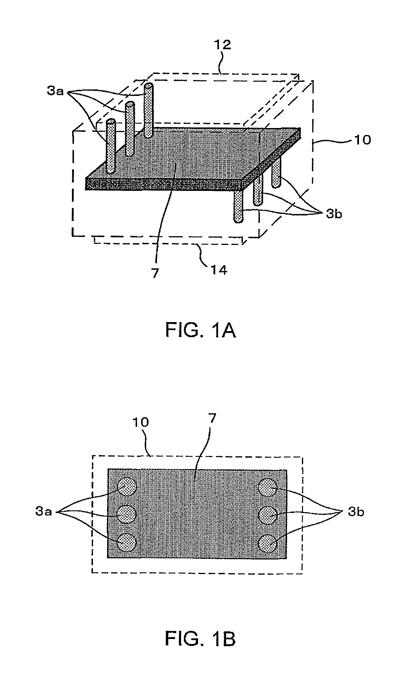
[0018]Embodiments according to the present invention are described in detail with reference to attached drawings. FIG. 1A and FIG. 1B are illustrations of a structure of a multilayer ceramic substrate, which is a laminated body, according to a first embodiment of the present invention. FIG. 1A is a perspective outline, and FIG. 1B schematically illustrates an internal structure of the multilayer ceramic substrate when seen from above. Here, although multilayer ceramic substrate types are not limited in particular, they are applicable to, for example, a multilayered circuit board etc. of low temperature co-fired ceramics (LTCC), which is a multilayer ceramic interconnection board with a multilayered circuit pattern in a resistor substrate.

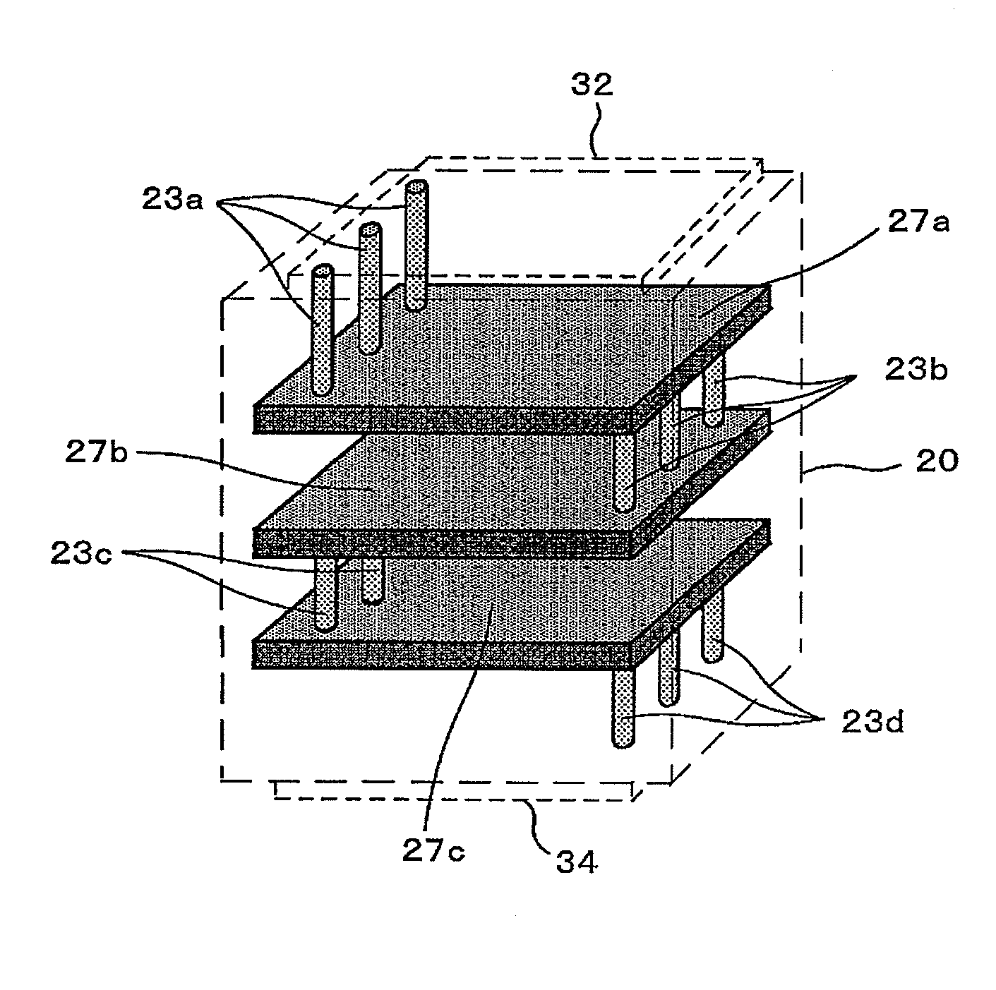
[0019]As shown in FIGS. 1A and 1B, with a multilayer ceramic substrate 10 according to the first embodiment, a resistive element 7 is arranged in a predetermined layer of the multiple layers comprising the substrate. Multiple via-electrodes 3a (thre...

second embodiment

[0036]A second embodiment according to the present invention is explained forthwith. FIG. 6A and FIG. 6B show a structure of a multilayer ceramic substrate according to a second embodiment of the present invention, wherein FIG. 6A is a perspective outline showing an internal structure of the multilayer ceramic substrate, and FIG. 6B schematically shows an internal structure of the ceramic multilayer substrate of FIG. 6A when seen from above.

[0037]With the multilayer ceramic substrate shown in FIGS. 6A and 6B, pad electrodes 105a and 105b are arranged facing each other on the substrate of a predetermined layer comprising a laminated body of a ceramic multilayer substrate (laminated body) 100, and a resistive element 107 bridges between these pad electrodes 105a and 105b. Multiple (three in the case shown in FIGS. 6A and 6B) via-electrodes 103a and 103b arranged in parallel are arranged on the pad electrodes 105a and 105b. With such a structure, one ends of the respective via-electrod...


PUM


Abstract

A laminated body and fabrication method thereof, which allow space saving and control of variation in internal layer resistance, are provided. When forming an internal-layer resistive element 7 in a multilayer ceramic substrate 10, the internal-layer resistive element 7 is connected to exterior electrodes (an upper surface electrode 32 and an undersurface electrode 34) via multiple via-electrodes 3a and 3b arranged in parallel, without a pad electrode adopted in the conventional laminated body. Moreover, in a multilayer ceramic substrate having multiple internal-layer resistive elements arranged in a multilayer structure, multiple internal-layer resistive elements are directly connected via multiple via-electrodes arranged in parallel.

Description

TECHNICAL FIELD[0001]The present invention relates to a laminated body, such as a multilayer ceramic substrate having internal resistors, for example, and a method for manufacturing the same.BACKGROUND ART[0002]A chip resistor mounted on small electronic equipment etc. has pad electrodes facing each other on an insulating substrate and a resistive element bridging between those pad electrodes. In such a resistor, when the resistive element is connected to an exterior electrode via a pad electrode, the area of the pad electrode is added to the area of the resistive element in a laminated body. Therefore, for example, a circuit board having a structure in which a resistive element is formed directly above a via-hole without preparing such an electrode, directly connecting it to the electric conductor in the via-hole has been proposed in Japanese Patent Application Laid-Open No. 6-77660.[0003]Since in a conventional chip resistor including a resistive element (resistive layer), a resis...

Claims


Application Information

Patent Timeline
Patent Type & Authority Patents(United States)
IPC IPC(8): H01C7/18
CPCH01C1/14H01C7/003H01C7/18H01C17/28H05K1/167H05K1/0306H05K1/115H05K3/4611H05K3/4629H05K2201/09672H05K2201/0979
Inventor TONOUCHI, ISAO
Owner KOA CORP
Why Eureka
Try Eureka