Supercharge Your Innovation With Domain-Expert AI Agents!

Array substrate for flat-panel display device and its manufacturing method

a flat-panel display and manufacturing method technology, applied in semiconductor devices, instruments, optics, etc., can solve the problems of insufficient repair, complicated repairing process, and decrease in the ratio of shippable goods among whole products

Inactive Publication Date: 2012-06-12
TOSHIBA MATSUSHITA DISPLAY TECH
View PDF5 Cites 1 Cited by
  • Summary
  • Abstract
  • Description
  • Claims
  • Application Information

AI Technical Summary

Benefits of technology

"The invention is a new design for an array substrate used in electronic devices. It includes a plurality of scanning lines, control lines, and signal lines arranged in a matrix form. The design also includes switching elements, insulator films, pixel electrodes, and metal patterns. The technical effect of this design is that it allows for easier repair of wire breakage on signal lines without causing short circuits with adjacent pixel electrodes."

Problems solved by technology

Such wire breakage causes a line defect on the screen, and thus may cause a decrease in a ratio of shippable goods among whole of products.
Such method requires a series of processes including a layer formation and a patterning; and thus repairing processes are complicated and sufficient decrease of the repairing is not achievable.
This method is not applicable when laser irradiation causes deterioration in a layer at underneath, such as an alteration in nature of a semiconductor layer.
This method has a further drawback in that the repair pattern is susceptible to short circuiting with neighboring pixel electrodes, when to repair a wire breakage on a signal line for example.
This is due to diffusion of laser beams and metals, which causes a certain thin metal layer around an intended area for forming the repair pattern and thereby causes short-circuiting with nearby pattern of conductive layer.
These conventional methods of repairing the wire breakage have a drawback in that unwanted short circuiting might be made between the repair pattern and neighboring pixel electrode because it is necessary to form the pair of contact holes by laser cutting and then form the bypass wiring.

Method used


Image

  • Array substrate for flat-panel display device and its manufacturing method
  • Array substrate for flat-panel display device and its manufacturing method
  • Array substrate for flat-panel display device and its manufacturing method

Examples


first embodiment

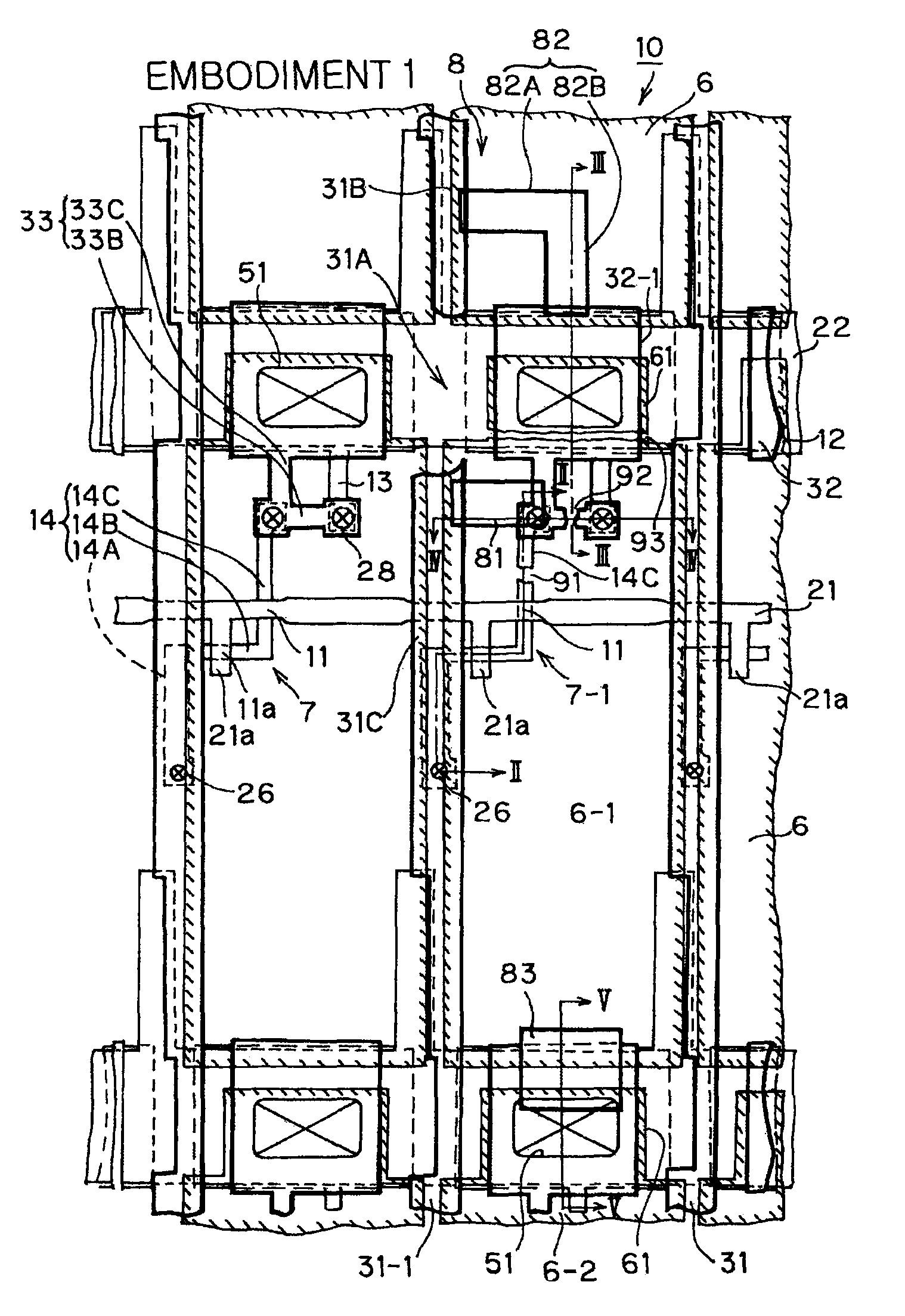
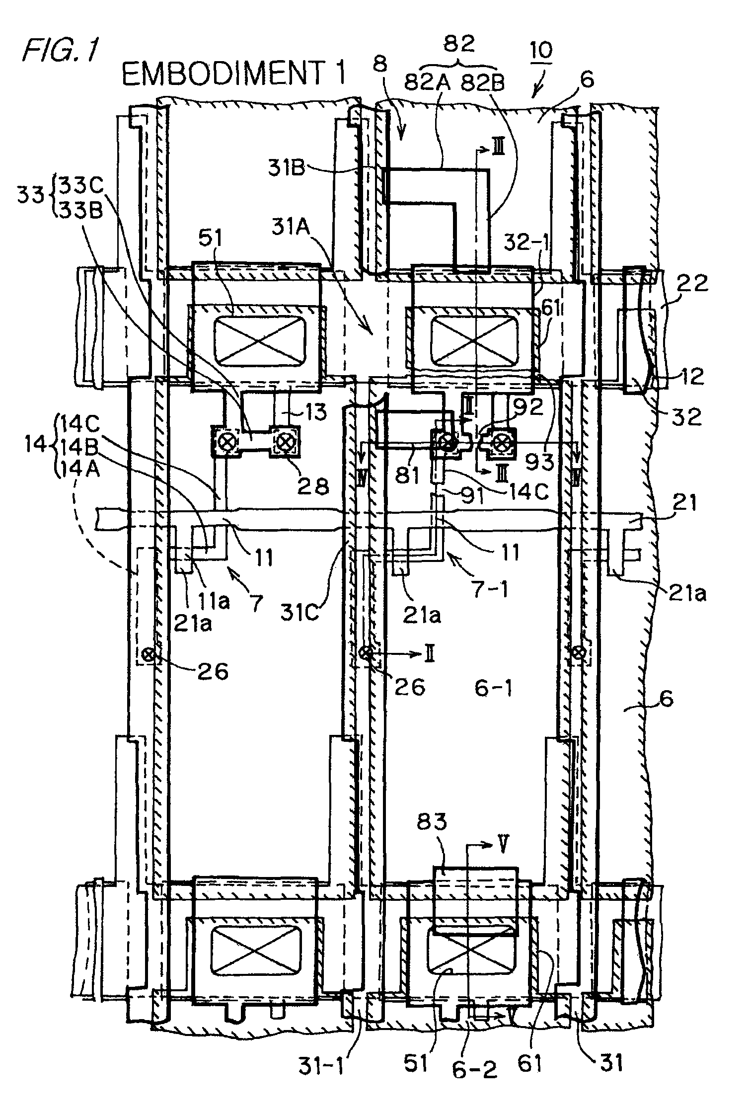
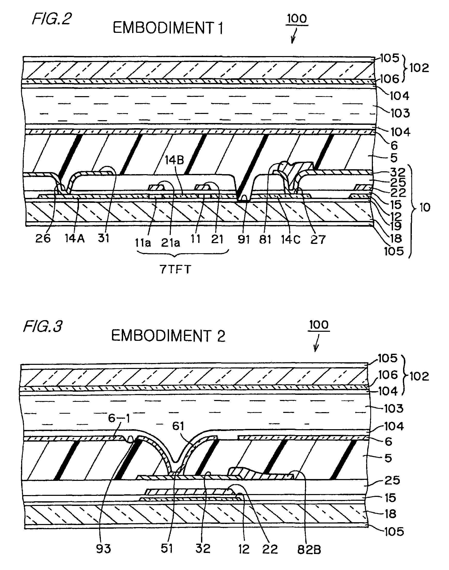
[0022]An array substrate and its manufacturing method of first embodiment of the invention will be described with reference to FIGS. 1 through 5. Exemplified in following explanation is an array substrate for a transmission liquid crystal display device, which has poly-crystalline silicone (p-Si: to be referred as polysilicone) TFTs for respective pixel electrodes as switching elements. The explanation is made for a case where a wire breakage 31A of one of signal lines 31 is occurred in a position at which the one signal line 31 crosses over a storage capacitor line 22, due to a foreign particle or the like at a time of lithographic exposure for forming a resist pattern, and is repaired.

[0023]FIG. 1 shows a construction of each pixel dot on the array substrate. Scanning lines 21 perpendicularly intersect signal lines 31 as to form a matrix or lattice form; and a TFT 7 is formed on each intersection of the scanning and signal lines. A storage capacitor (Cs) line 22 having a relativel...

second embodiment

[0047]Second embodiment of the invention will be explained by use of a plan view of FIG. 6 that corresponds to FIG. 1. This embodiment is to cope with an occasion where not only the wire breakage 31A on the signal line 31 but also a wire breakage 33A on a proximal or base portion of the L-shaped extension 33 are formed. In such occasion, it is easier to arrange the bypass wiring 8 on a side opposite to that of the first embodiment. In other words, instead of using the metal island pattern 32-1 on the pixel dot associated with the one signal line 31-1 having the wire breakage 31A, it is adopted for the bypass wiring 8, the metal island pattern 32-2 on a next pixel dot that is demarcated, by the one signal line 31-1 having the wire breakage 31A, from the pixel dot associated with the one signal line 31-1. In other words, the metal island pattern 32-2 used here has not been supplied with signal from the one signal line 31-1 having the wire breakage 31A; and is another one among the two...


PUM

PropertyMeasurementUnit
thicknessaaaaaaaaaa
thicknessaaaaaaaaaa
thicknessaaaaaaaaaa

Abstract

An array substrate comprising: a first insulator film arranged to insulate scanning and control lines from signal lines; switching elements, each of which is arranged in vicinity of respective intersection of the scanning and signal lines; a second insulator film that covers a multi-layer wiring pattern including the scanning and control lines and the signal lines; pixel electrodes, each of which is electrically connected to respective one of the signal lines through the respective switching element; island metal patterns, each of which is arranged to at least partly overlap the control line and is electrically connected with the respective switching element; a wiring breakage that separates one of the signal lines into two wiring parts; and bridge wirings, which connect said two wiring parts by way of one of the island metal patterns and are arranged to overlap the pixel electrodes as interposed by the second insulator film therebetween.

Description

CROSS-REFERENCE TO RELATED APPLICATION[0001]This application is based upon and claims the benefit of priority from the prior Japanese Patent Application No. 2007-225454, filed on Aug. 31, 2007; the entire contents of which are incorporated herein by reference.FIELD OF THE INVENTION[0002]This invention relates to an array substrate used in a flat-panel display device, as typified by a liquid-crystal display (LCD) device and Organic Electro-Luminescence (OEL or OLED) display device, and a manufacturing method of the array substrate. The invention particularly relates to the array substrate having been undergone repairing of wire breakage as to curb a line defect on a screen, which would be caused by a wire breakage in a pixel-array area.BACKGROUND ART[0003]Recently, liquid crystal display devices and other flat-panel display devices are used in various fields as image display devices for personal computers, word processor-dedicated machines, television set or the like as well as for a...

Claims


Application Information

Patent Timeline
Patent Type & Authority Patents(United States)
IPC IPC(8): G02F1/1333G02F1/1343
CPCG02F1/136259G09G3/20H01L27/124G02F2001/136263G09G2300/0426G09G2330/08G09G3/3648G02F1/136263
Inventor IMAI, NOBUO
Owner TOSHIBA MATSUSHITA DISPLAY TECH
Features
  • R&D
  • Intellectual Property
  • Life Sciences
  • Materials
  • Tech Scout
  • Unparalleled Data Quality
  • Higher Quality Content
  • 60% Fewer Hallucinations
Learn More