Data driver for display device, test method and probe card for data driver

a data driver and display device technology, applied in static indicating devices, instruments, optics, etc., can solve the problems of high possibility of breakage caused by foreign matter in a fabricating process or deficiency in a lithographic process, and the inability to drive pixels arranged forward of the broken portion, so as to achieve the effect of determining quality

Inactive Publication Date: 2012-07-10
RENESAS ELECTRONICS CORP
View PDF8 Cites 3 Cited by
  • Summary
  • Abstract
  • Description
  • Claims
  • Application Information

AI Technical Summary

Benefits of technology

[0040]According to a data driver according to a display device of the present invention, when a test mode is conducted, the switches 60-1, 60-2 supply the drive signals (the output gray-scale voltages) to the inputs of the repair amplifiers 40-1, 40-2. As a consequence, an amplitude value of the analog voltage (the output gray-scale voltages) equivalent to that in the test of the output delay of the normal amplifiers 36, 36-1 to 36-n is inputted into the inputs of the repair amplifiers 40-1, 40-2. Therefore, the outputs of the repair amplifiers 40-1, 40-2 can be subjected to a test equivalent to that of the output delay of the amplifiers 36, 36-1 to 36-n. Thus, it is possible to precisely determine the quality with using a mass-produced LSI tester 55 based on the output delays of the repair amplifiers 40-1, 40-2.

Problems solved by technology

As a result, the possibility of breakage caused by foreign matters in a fabricating process or deficiency in a lithographic process bas been becoming high.
If a signal line is broken when the driver outputs the drive signal for driving the signal line, the pixels arranged forward of the broken portion cannot be driven.
In this case, the display device results in a defective device.
One can find this deficiency only when an electric test is conducted at the final stage at which the panel is fabricated and the driver, the substrate and the like are connected and assembled, so that a vast cost occurs when a deficiency is found out.
However, in the case of performing an electric characteristics inspection of the repair amplifiers 40-1 and 40-2, there arises a problem that, when the quality of the output delay of the repair amplifiers 40-1, 40-2 is judged, the quality cannot be judged similarly to the output delay of the n amplifier 36-1 to 36-n in the amplifier circuit 36 because of the specifications of the tester.
However, it is difficult to reproduce the output switch in the DAC 35 by the input from the mass-produced LSI tester 55, because of limitation of the ability or the cost of the tester 55.
Furthermore, in some cases, there is a limitation of the maximum input analog voltage of the test device from the viewpoint of the cost of the mass-produced LSI tester 55.
That is to say, there arises a problem that the quality of the repair amplifiers 40-1 and 40-2 cannot be precisely determined by tests using mass-produced products.

Method used


Image

  • Data driver for display device, test method and probe card for data driver
  • Data driver for display device, test method and probe card for data driver
  • Data driver for display device, test method and probe card for data driver

Examples


first embodiment

(First Embodiment)

[Configuration]

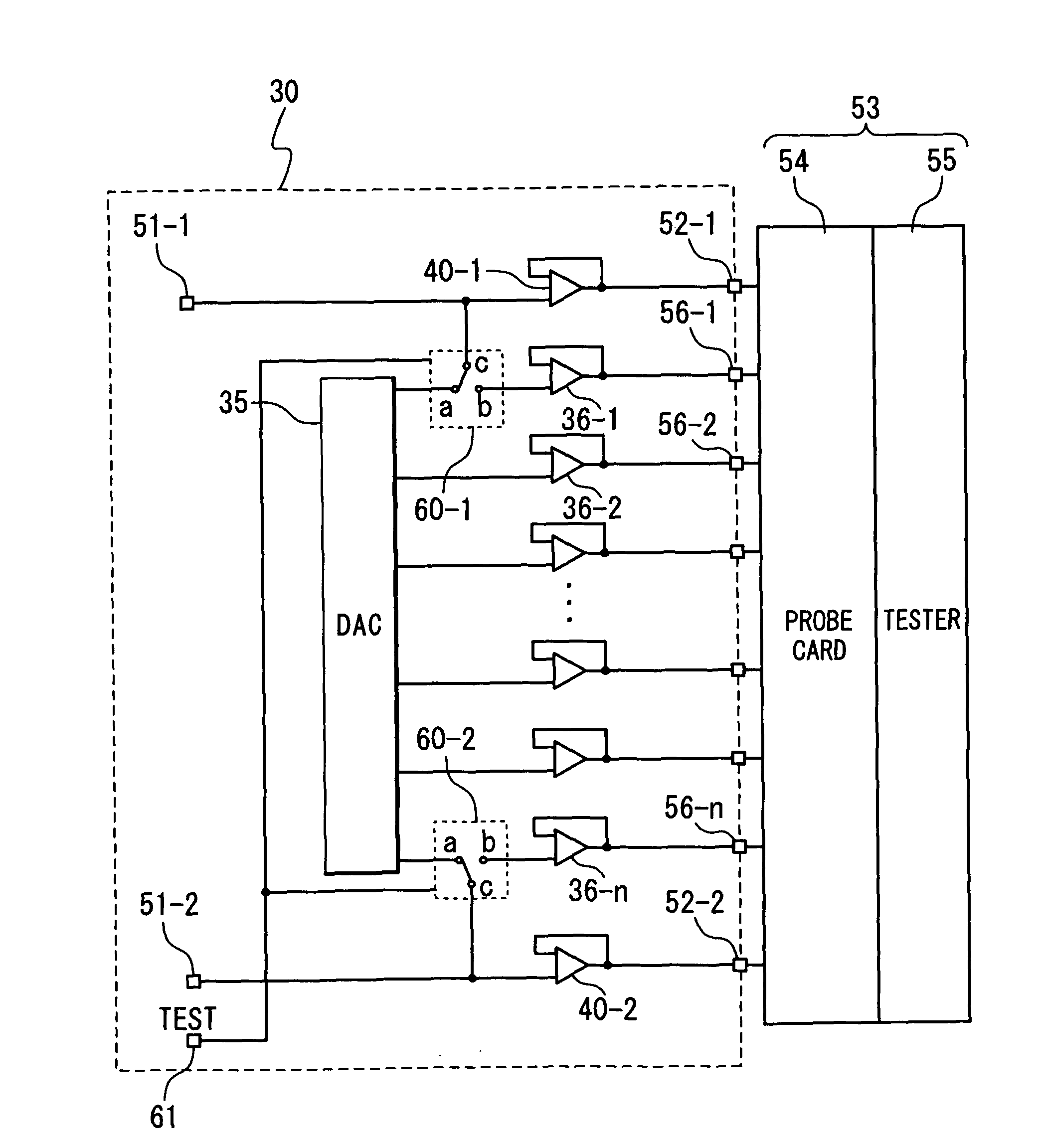
[0052]FIG. 6 illustrates a configuration of a data driver 30 of a TFT type liquid crystal display device 1 and measurement equipment 53 which is connected to the data driver 30 and includes a probe card 54 and a tester 55 in a first embodiment according to the present invention. The data driver 30 is provided with switches 60-1 and 60-2 and a testing pad 61. The switches 60-1 and 60-2 and the testing pad 61 are mounted on a chip. The measurement equipment 53 including the probe card 54 and the tester 55 is connected to the chip when an electric characteristics inspection, described later, is conducted.

[0053]The testing pad 61 is connected to the switches 60-1 and 60-2 via wirings. Repair amplifiers 40-1 and 40-2 are disposed in respective vicinities of amplifiers 36-1 and 36-n, in an amplifier circuit 36 inside of the data driver 30. The switches 60-1 and 60-2 are interposed between a DAC 35 inside of the data driver 30 and the amplifiers 36-1 and 36...

second embodiment

(Second Embodiment)

[Configuration]

[0060]FIG. 7 illustrates a configuration of the data driver 30 of a TFT type liquid crystal display device 1 according to a second embodiment of the present invention and measurement equipment 53 which is connected to the data driver 30 and includes the probe card 54 and the tester 55. The data driver 30 is provided with switches 60-1 and 60-2, a testing pad 61 and auxiliary DACs 70-1 and 70-2. The switches 60-1 and 60-2, the testing pad 61 and the auxiliary DACs 70-1 and 70-2 are mounted on a chip. The measurement equipment 53 including the probe card 54 and the tester 55 is connected to the chip when an electric characteristics inspection is conducted.

[0061]The testing pad 61 is connected to the switches 60-1 and 60-2 and the auxiliary DACs 70-1 and 70-2 via wirings. Repair amplifiers 40-1 and 40-2 are disposed in respective vicinities of amplifiers 36-1 and 36-n, in an amplifier circuit 36 inside of the data driver 30. The switches 60-1 and 60-2 ...

third embodiment

(Third Embodiment)

[Configuration]

[0069]FIG. 8 illustrates a configuration of a data driver 30 in a TFT type liquid crystal display device 1 and measurement equipment 53, which is connected to the data driver 30 and includes the probe card 54 and the tester 55, according to a third embodiment of the present invention. The measurement equipment 53 including the probe card 54 and the tester 55 is connected to the chip when an electric characteristics inspection is conducted. The probe card 54 includes switches 60-1 and 60-2 and testing wirings 80-1 and 80-2.

[0070]Repair amplifiers 40-1 and 40-2 are disposed in respective vicinities of amplifiers 36-1 and 36-n in an amplifier circuit 36 inside of the data driver 30. The switches 60-1 and 60-2 are interposed between output pads 56-1 and 56-n and the tester 55, respectively, on the probe card 54. Each of the switches 60-1 and 60-2 includes a terminal “a” connected to an output of each of the output pads 56-1 and 56-n, a terminal “b” conne...


PUM


Abstract

A data driver of a display device includes: a DAC (Digital Analog Converter) outputting a drive signal for driving a signal line of a displaying unit; an amplifier amplifying the drive signal outputted by the DAC and outputting the drive signal to the signal line; a repair amplifier having an input and an output, wherein the signal line is separated by a breakage point into a connected data line connected to the amplifier and a disconnected data line not connected to the amplifier, and the input of the repair amplifier is connected to the connected data line and the output of the repair amplifier is connected to the disconnected data line; and a switch supplying the drive signal to the input of the repair amplifier for testing the repair amplifier. An output delay test for the repair amplifier can be performed under a condition similar to that of the amplifier.

Description

INCORPORATION BY REFERENCE[0001]This patent application is based on Japanese Patent Application No. 2007-180083. The disclosure of the Japanese Patent Application is incorporated herein by reference.BACKGROUND OF THE INVENTION[0002]1. Field of the Invention[0003]The present invention relates to a data driver of a display device, a test method and a probe card for the data driver and, more particularly, to a technique suitable for testing a repair amplifier of a data driver.[0004]2. Description of Related Art[0005]Flat panel displays become widely used in recent years. There are various types of flat display panels such as the TFT (abbreviating “a Thin Film Transistor”) type liquid crystal display device, the simple matrix type liquid crystal display device, the electroluminescence (abbreviated as “EL”) display device and the plasma display device. On a display (i.e., a screen) of the display device, display data are displayed. In the following, the TFT type liquid crystal display is...

Claims


Application Information

Patent Timeline
Patent Type & Authority Patents(United States)
IPC IPC(8): G09G5/00
CPCG09G3/006G09G3/3688G09G2310/027G09G2310/0291G09G2330/08G09G2330/12
Inventor MATSUI, TADAYOSHI
Owner RENESAS ELECTRONICS CORP
Why Eureka
Try Eureka